


Problems and solutions for substrates in PCB design
1. Various soldering problems
It is now a symbol: there are blast holes in cold solder joints or solder joints.
Inspection method: The hole is often analyzed before and after dip soldering to find the place where the copper is stressed. In addition, the raw material is subjected to the feed inspection.
Possible cause: The blast hole or cold solder joint is seen after the soldering operation. In many cases, the copper plating is poor, and then expansion occurs during the soldering operation, causing holes or blast holes in the metallized hole walls. If this is produced during the wet processing process, the absorbed volatiles are masked by the coating and then driven out under the heat of the dip soldering, which creates a spout or blasthole.
Solution: Try to eliminate copper stress. The expansion of the laminate in the z-axis or thickness direction is generally related to the material. It can cause the metallized holes to break. Work with laminate manufacturers to get advice on materials with smaller z-axis expansion.
2. Bond strength problem
It is now a symbol: in the dip soldering process, the pads and wires are detached.
Inspection method: During the feed inspection, fully test and carefully control all wet processing processes.
possible reason:
1. The delamination of the pads or wires during processing may be due to plating solution, solvent etch or copper stress during the plating operation.
2. Punching, drilling or perforating will cause the pad portion to detach, which will become apparent during the hole metallization operation.
3. During wave soldering or manual soldering operations, pad or wire detachment is usually caused by improper soldering or excessive temperature. Sometimes the laminate or wire is detached because the laminate is not properly bonded or the thermal peel strength is not high.
4. Sometimes the design routing of the printed board can cause the pads or wires to detach in the same place.
5. During the soldering operation, the retained heat of absorption of the component causes the pad to detach.
Solution:
1. Give the laminate manufacturer a complete list of solvents and solutions, including the processing time and temperature for each step. Analyze whether the plating process has copper stress and excessive thermal shock.
2. Obey the mechanical processing methods of push storage. The metallized holes are often analyzed to control this problem.
3. Most of the pads or wires are disconnected due to the lack of strict requirements for all operators. The failure of the temperature check of the solder bath or the extension of the residence time in the solder bath can also occur. In the manual soldering trimming operation, the pad detachment is probably due to the improper use of wattage.
Electric ferrochrome, and the failure to carry out professional process training. Some laminate manufacturers now use laminates that have high levels of peel strength at elevated temperatures for use in stringent soldering.
4. If the detachment caused by the design wiring of the printed board occurs in the same place on each board; then the printed board must be redesigned. Usually, this does happen in thick copper foil or wire corners. Sometimes, long wires can also happen like this; this is because
It is due to the difference in thermal expansion coefficient.
5 PCB design time. When possible, remove heavy components from the entire printed board or install them after dip soldering. It is usually carefully soldered with a low wattage soldering iron, which is shorter than the component dip soldering.
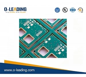
PCB Assembly manufacturer china
3. Oversize change problem
It is now a symbol: the size of the substrate is out of tolerance or misaligned after processing or soldering.
Inspection method: Full quality control during processing.
possible reason:
1. The direction of the texture of the paper-based material is not noticed, and the forward expansion is about half of the transverse direction. Moreover, the substrate cannot be restored to its original size after cooling.
2. The local stress in the laminate, if not released, sometimes causes irregular dimensional changes during processing.
Solution:
1. The entire production staff often cuts the sheet in the same structural texture direction. If the dimensional change is outside the allowable range, consider using a substrate instead.
2. Contact the laminate manufacturer for advice on how to release material stress prior to processing.