


- Contact Us
-
TEL: + 86-13428967267
FAX: + 86-4008892163-239121
+ 86-2028819702-239121
Email: sales@o-leading.com Contact Now
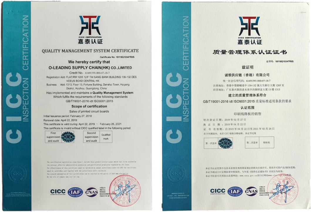
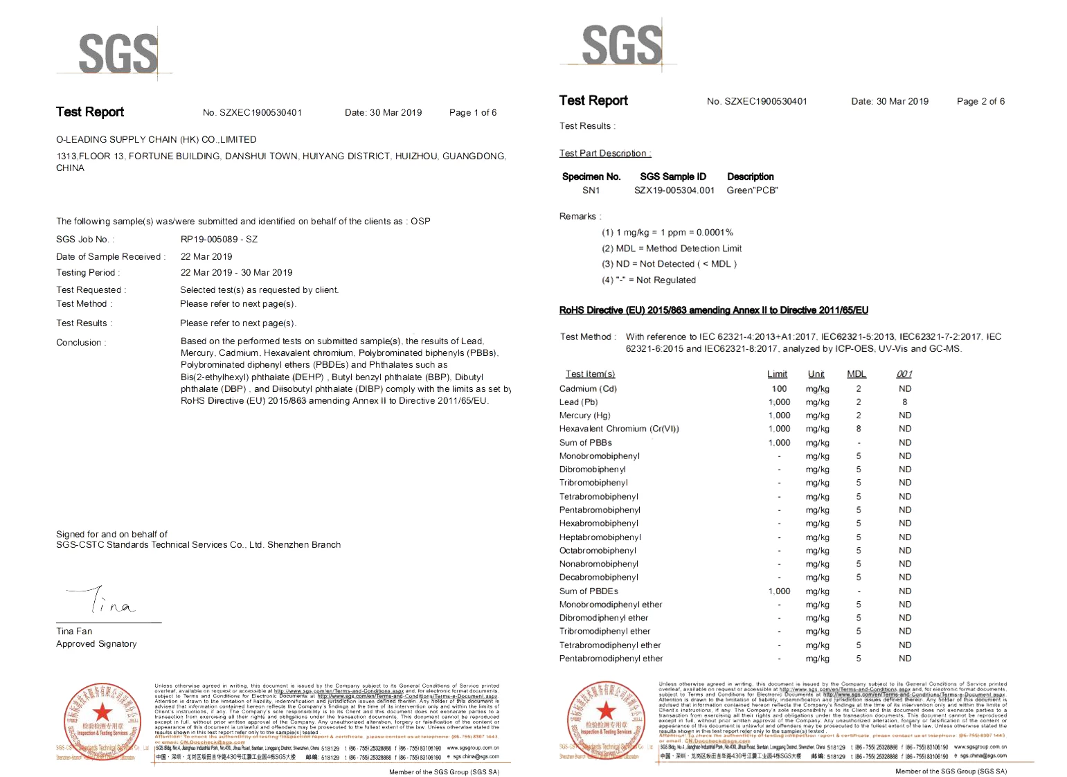
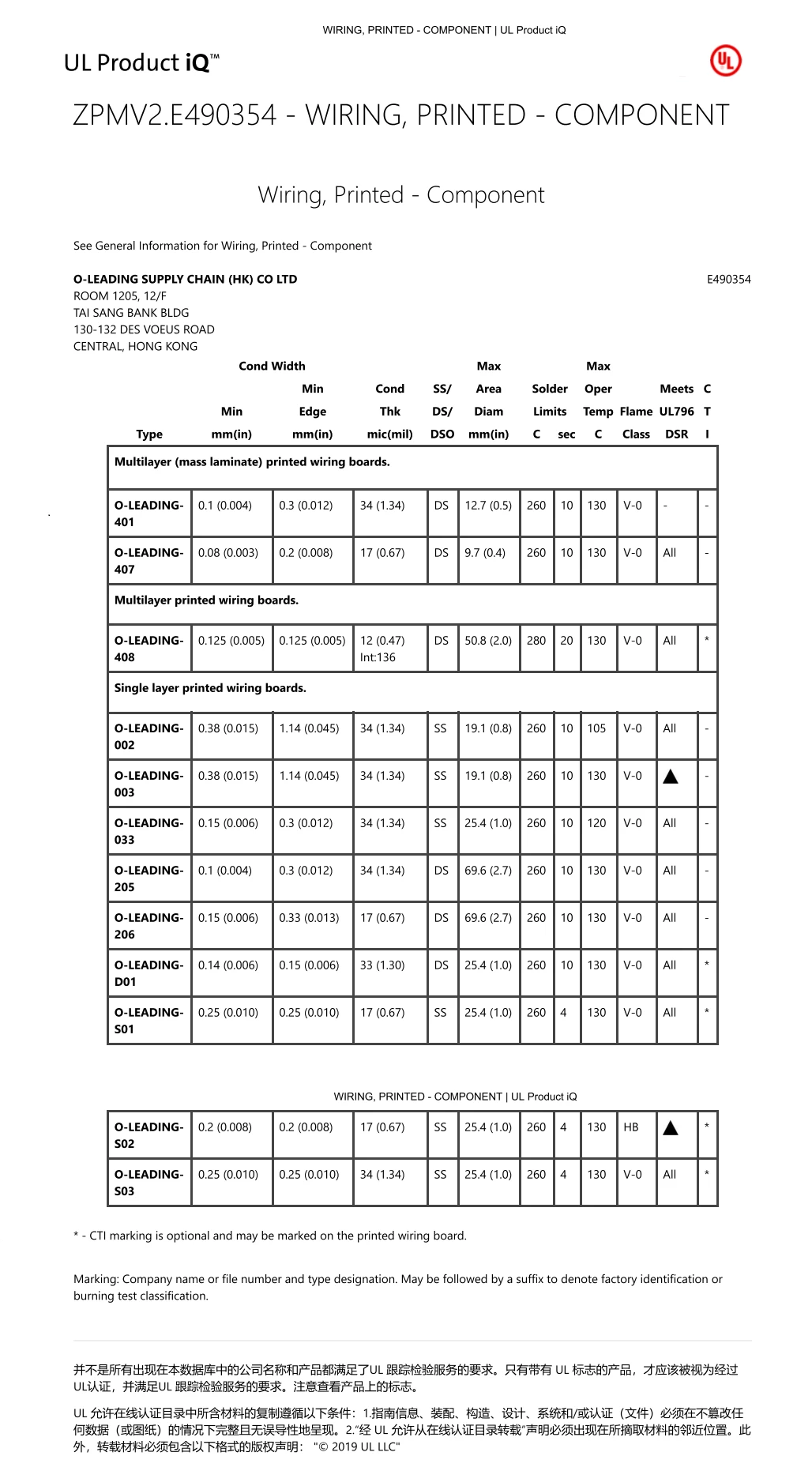
- Certifications
-


- Subscribe
-
Get email updates on new products
- New Products


- Electronic album

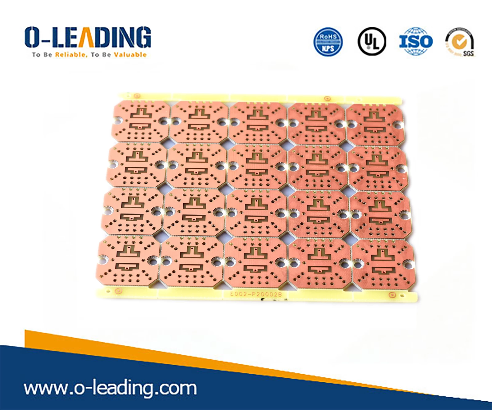
Golden PCB manufacturer Fingers China, hard gold plating supplier, Prototype PCB Assembly company china
- P / N PCB: LE-500V1
- Counting layers: 1L
- Material: basic aluminum.
- Board: 1.6 mm
- copper thk: 1 oz
- Smallest hole size: 2.0 mm
- Number of holes (pcs): 16
- line without: 20 / 20mil
- Y / N impedance check (Tol%): N
| Welcome to O-leading |
We are professional PCB manufacturers with more than ten years experience. Product range: single, double side, multilayer PCB, flexible PCB and MCPCB. We can provide a rapid prototyping service: S / S in 24 hours, 4-8 units in 48-96 hours of production.
COPPER PLATE HOLES MINIMUM .025 AVG, .020 MIN .. HOLES CAN NOT BE CONNECTED
Package with colorless transparent bubble film, 25 pieces / bag, put the desiccant on the side, put the humidity indicator board on the upper side
CLICK THIS FOR FURTHER INFORMATION:
| Product description |
| PCB P / N | LE-500V1 |
| Counting layers | 1L |
| Material | Basic ceramics |
| Board of Directors | 1.6 mm |
| thk of copper | 1 oz |
| Smallest hole size | 2.0 mm |
| Number of holes (pcS) | 16 |
| line w /S | 20 / 20mil |
| S / N impedance check (Tol%) | N |
| Surface finish | ENIG (Au: 0.05um) |
| Silkscreen welding mask | White black |
| Single dimensions | Dim X (mm): Dim X (mm): 100; Dim Y (mm): 115 |
| Panelisation | Dim X (mm): 100; Dim Y (mm): 115; UPS no: 1 |
| Special: peelable mask | N |
| Routing / Punching | Countersunk CNC screw + |

| FAQ |
1. How does O-Leading guarantee quality? Supplier of hard gold plating
Our high quality standard is obtained with the following.
1. The process is strictly controlled according to ISO 9001: 2008 standards.
2. Extensive use of software in the management of the production process
3. Cutting-edge testing tools and tools. For example. Flying Probe, X-ray Inspection, AOI (Automated Optical Inspector) and ICT (in-circuit test).
4. Specified quality assurance team with failure case analysis process
5. Training and continuous training of personnel
2. How does O-Leading keep the competitive price?
In the last decade, the prices of many raw materials (eg copper, chemicals) had doubled, tripled or quadrupled; The RMB Chinese currency had appreciated 31% against the US dollar; And our labor costs have also increased significantly. However, O-Leading has kept our prices constant. This is all about our innovations in reducing costs, avoiding waste and improving efficiency. Our prices are very competitive in the industry at the same level of quality.
We believe in a win-win partnership with our customers. Our partnership will be mutually beneficial if we are able to provide you with an advantage in terms of cost and quality.
3. What types of cards can the O-Leading process use?
FR4 common, high TG and halogen-free boards, Rogers, Arlon, Telfon, aluminum / copper boards, PI, etc.
4. What data are needed for PCB production?
It is better to provide data in the Gerber 274-X format. In addition, Cam350, CAD, Protel 99se, PADS, DXP and Eagle can also be processed.
5. What is the typical process flow for multilayer PCBs?
Cutting material → Internal dry film → Internal etching → Internal AOI → Multi-bond → Layer overlapping Pressing → Drilling → PTH → Plating → External dry film → Plating → External engraving → External AOI → Welding mask → Component mark → Finishing surface → Routing → E / T → Visual inspection.
| Our Team |
| Certifications |
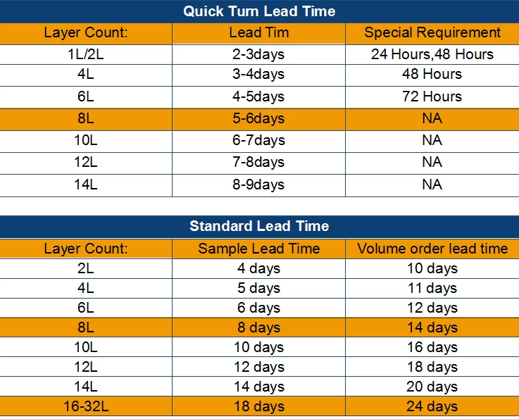
| Packaging & Delivery |

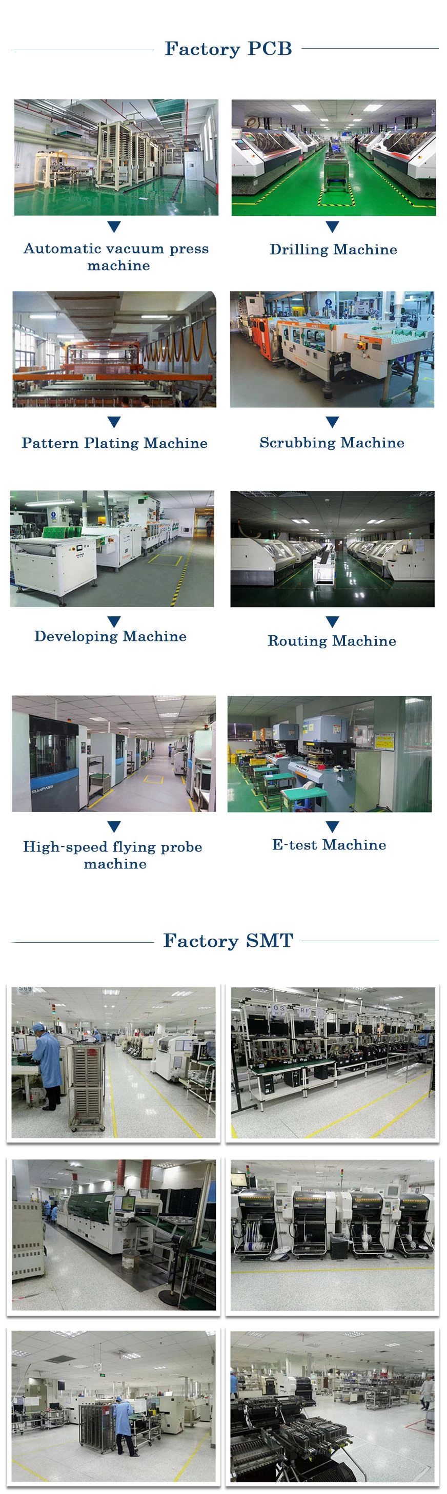
| Process Capability |
PCB Production Capabilities
Layer Count: 1Layer-32Layer
Finished copper thickness: 1/3oz-12oz
Min Line width/spacing internal: 3.0mil/3.0mil
Min Line width/spacing external: 4.0mil/4.0mil
Max Aspect Ratio: 10:1
Board thickness: 0.2mm-5.0mm
Max Panel size(inches): 635*1500mm
Minimum Drilled Hole Size: 4mil
PIated Hole Tolerance: +/-3mil
BIind/Buried Vias (AII Types): YES
Via Fill(Conductive,Non-Conductive): YES
Base Material: FR-4,FR-4high Tg.Halogen free material,Rogers,Aluminium base,Polyimide,
Heavy Copper
Surface finishes: HASL,OSP,ENIG,HAL-LF,lmmersion silver,lmmersion Tin,Gold fingers,Carbon ink
SMT Production Capabilities
PCB Material: FR-4,CEM-1,CEM-3,Aluminum-based board
Max PCB size: 510x460mm
Min PCB size:50x50mm
PCB Thickness:0.5mm-4.5mm
Board thickness:0.5-4mm
Min Components size: 0201
Standard chip size component: 0603 and larger
Component max height:15mm
Min lead pitch: 0.3mm
Min BGA ball pitch:0.4mm
Placement precision: +/-0.03mm


