


- Contact Us
-
TEL: + 86-13428967267
FAX: + 86-4008892163-239121
+ 86-2028819702-239121
Email: sales@o-leading.com Contact Now
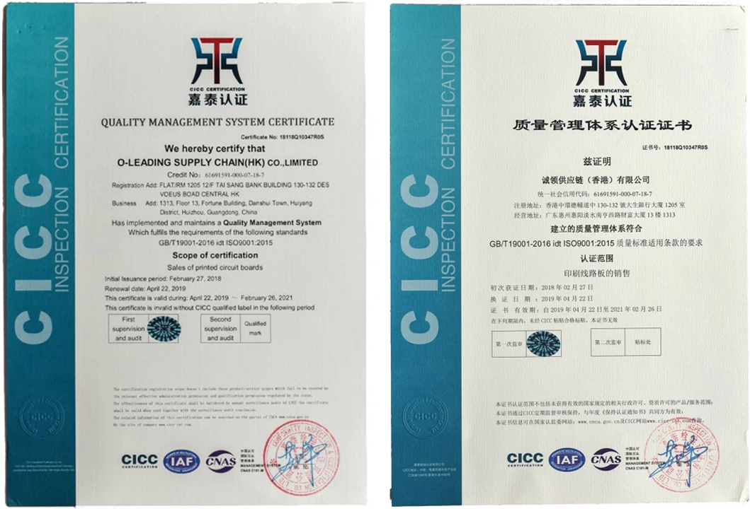
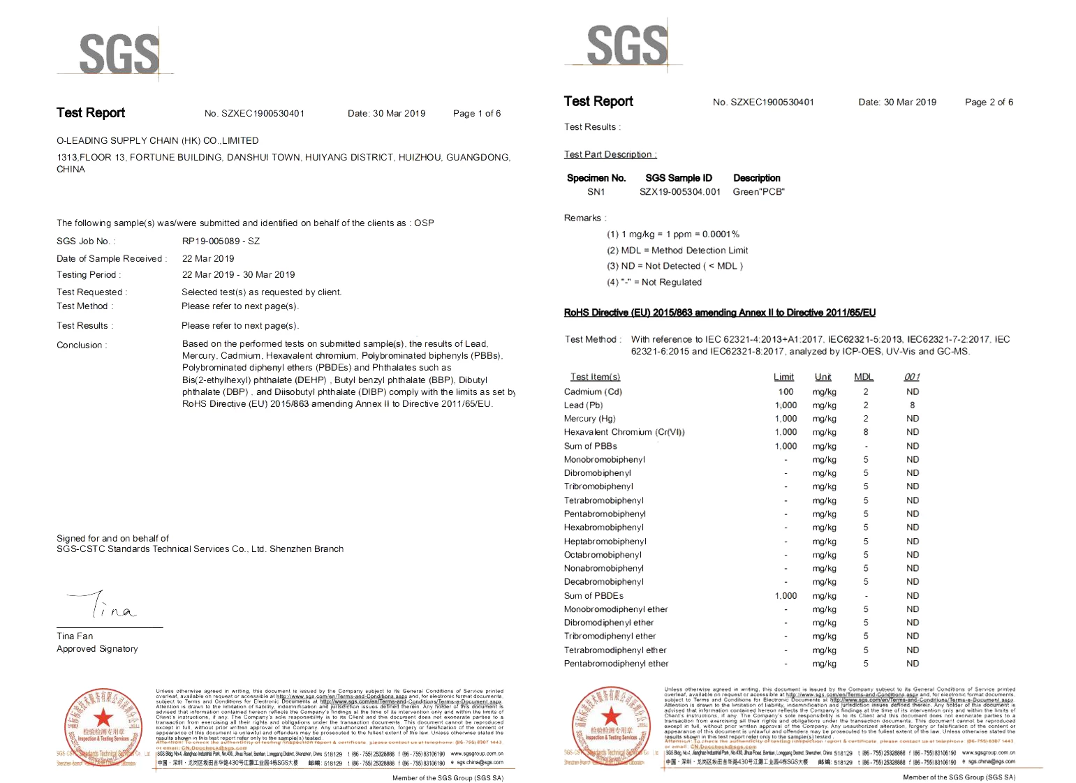
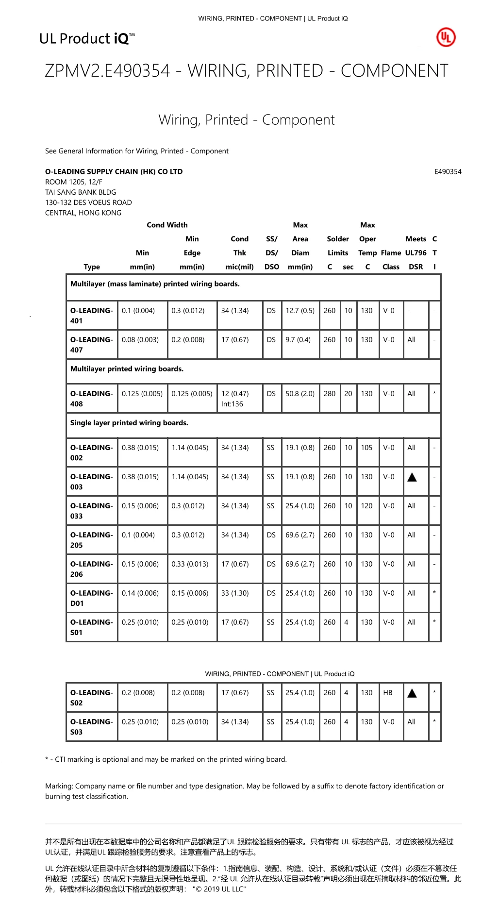
- Certifications
-


- Subscribe
-
Get email updates on new products
- New Products


- Electronic album

Ceramic PCB manufacturer china, High Temperature PCB supplier china, printed circuit boards supplier
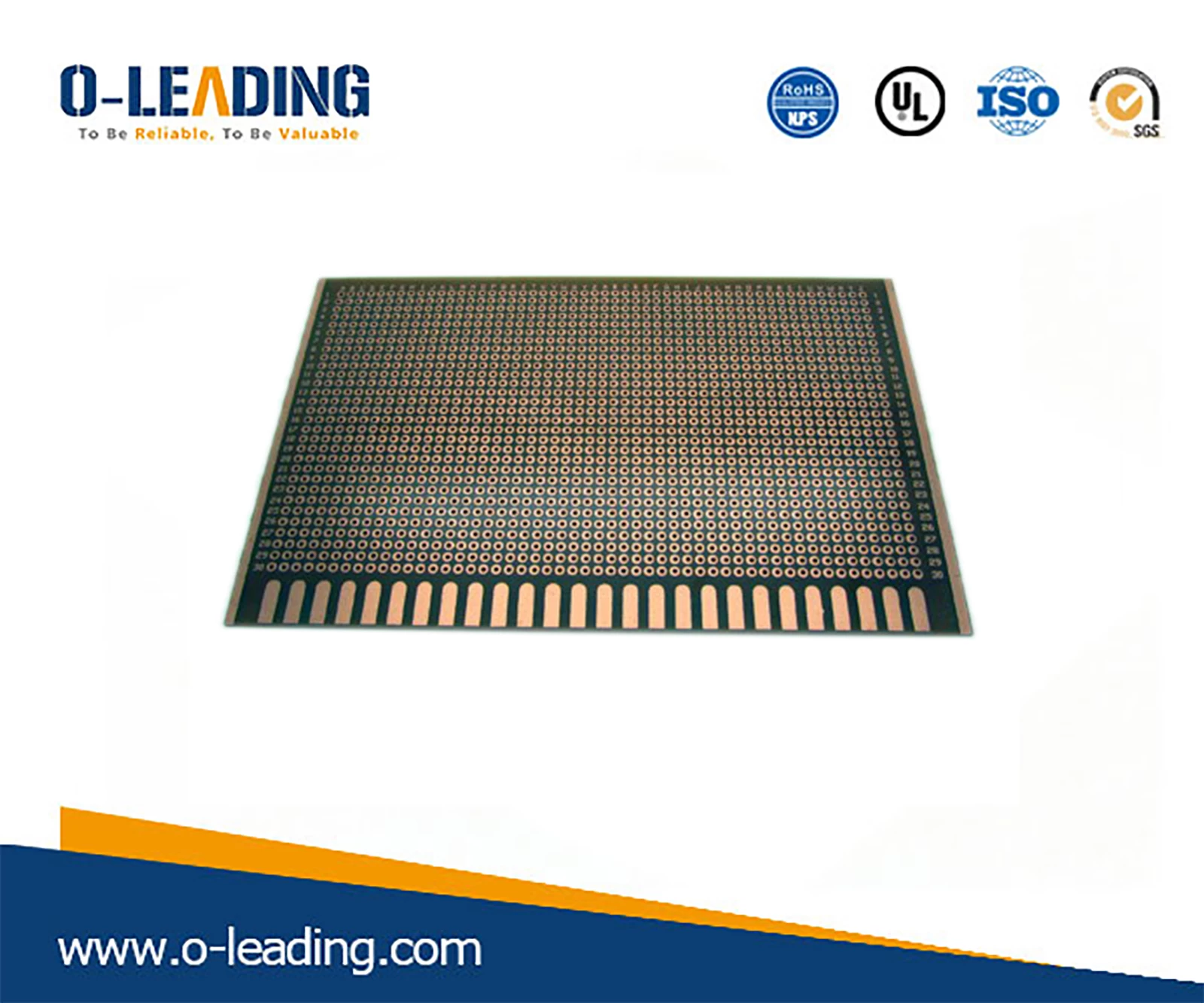
- P / N PCB: O-LEADING 150
- Counting layers: 1L
- Material: base Cu.
- Board thk: 3.2 mm
- copper thk: 1 oz
- Smallest hole size: /
- Number of holes (pieces): /
- line w / s: /
- Y / N impedance check (Tol%): N
| Welcome to O-leading |
We are professional PCB manufacturers with more than ten years experience. Product range: single, double side, multilayer PCB, flexible PCB and MCPCB. We are able to provide a rapid prototyping service: S / S in 24 hours, 4-8 units in 48-96 production hours. (printed circuit boards supplier)
COPPER PLATE HOLES MINIMUM .025 AVG, .020 MIN .. HOLES CAN NOT BE CONNECTED
Packaging with colorless transparent bubble film, 25 pieces / bag, put the desiccant on the side, put the humidity indicator on the upper side
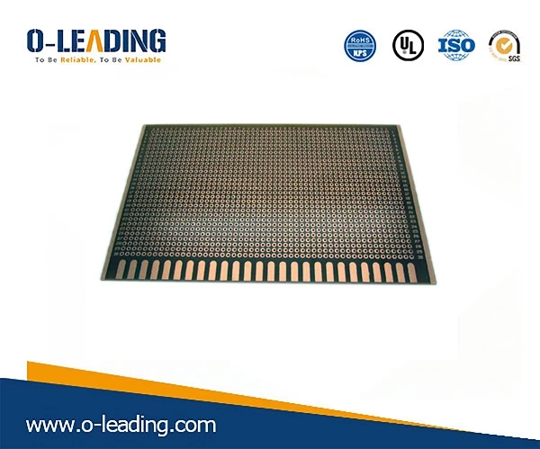
| Product description |
| PCB P / N | LE-150 |
| Counting layers | 1L |
| Material | Basic ceramics |
| Board of Directors | 3.2 mm |
| thk of copper | 1 oz |
| Smallest hole size | / |
| Number of holes (pieces) | / |
| line w / s | / |
| S / N impedance check (Tol%) | N |
| Surface finish | ENIG (Au: 0.05um) |
| Silkscreen welding mask | Black White |
| Single dimensions | Dim X (mm): 27; Dim Y (mm): 45 |
| Panelisation | Dim X (mm): 27; Dim Y (mm): 135; UPS no: 3 |
| Special: peelable mask | N |
| Routing / Punching | Countersunk CNC head screw + |
| Our Team |
| Certifications |
| Packaging & Delivery |

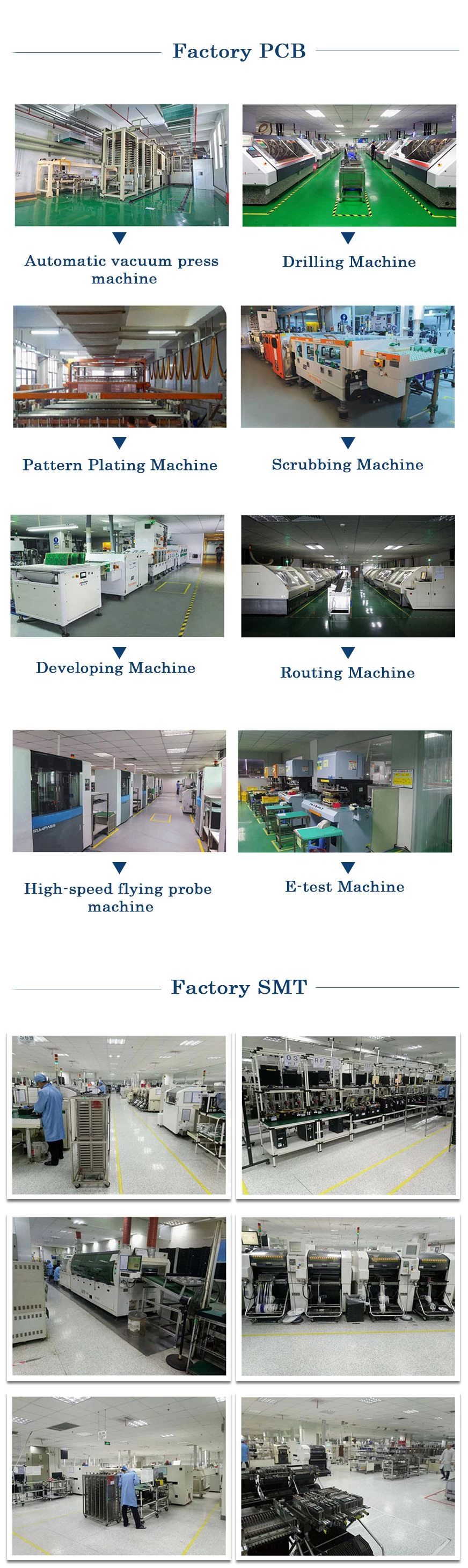
| Process Capability |
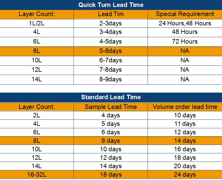
PCB Production Capabilities
Layer Count: 1Layer-32Layer
Finished copper thickness: 1/3oz-12oz
Min Line width/spacing internal: 3.0mil/3.0mil
Min Line width/spacing external: 4.0mil/4.0mil
Max Aspect Ratio: 10:1
Board thickness: 0.2mm-5.0mm
Max Panel size(inches): 635*1500mm
Minimum Drilled Hole Size: 4mil
PIated Hole Tolerance: +/-3mil
BIind/Buried Vias (AII Types): YES
Via Fill(Conductive,Non-Conductive): YES
Base Material: FR-4,FR-4high Tg.Halogen free material,Rogers,Aluminium base,Polyimide,
Heavy Copper
Surface finishes: HASL,OSP,ENIG,HAL-LF,lmmersion silver,lmmersion Tin,Gold fingers,Carbon ink
SMT Production Capabilities
PCB Material: FR-4,CEM-1,CEM-3,Aluminum-based board
Max PCB size: 510x460mm
Min PCB size:50x50mm
PCB Thickness:0.5mm-4.5mm
Board thickness:0.5-4mm
Min Components size: 0201
Standard chip size component: 0603 and larger
Component max height:15mm
Min lead pitch: 0.3mm
Min BGA ball pitch:0.4mm
Placement precision: +/-0.03mm
- Other Products


