


- Contact Us
-
TEL: + 86-13428967267
FAX: + 86-4008892163-239121
+ 86-2028819702-239121
Email: sales@o-leading.com Contact Now
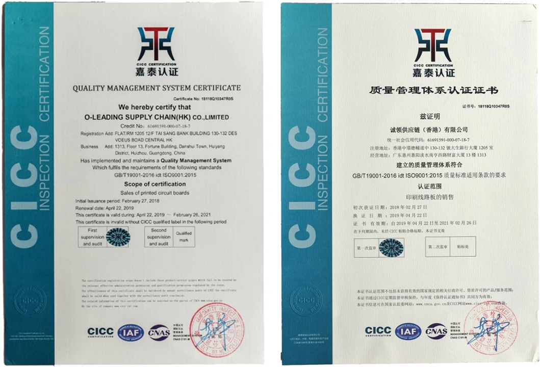
- Certifications
-


- Subscribe
-
Get email updates on new products
- New Products


- Electronic album

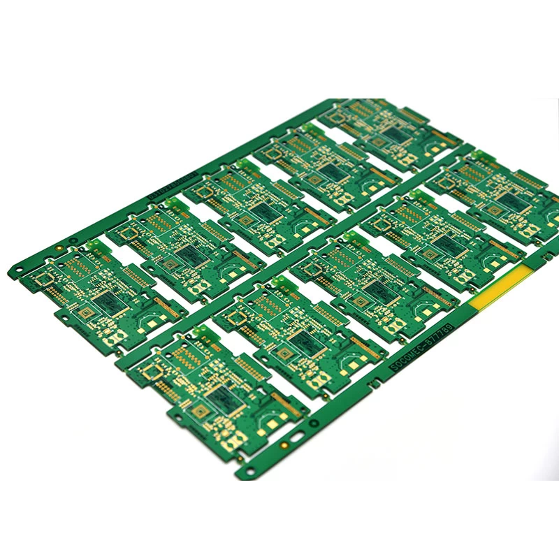


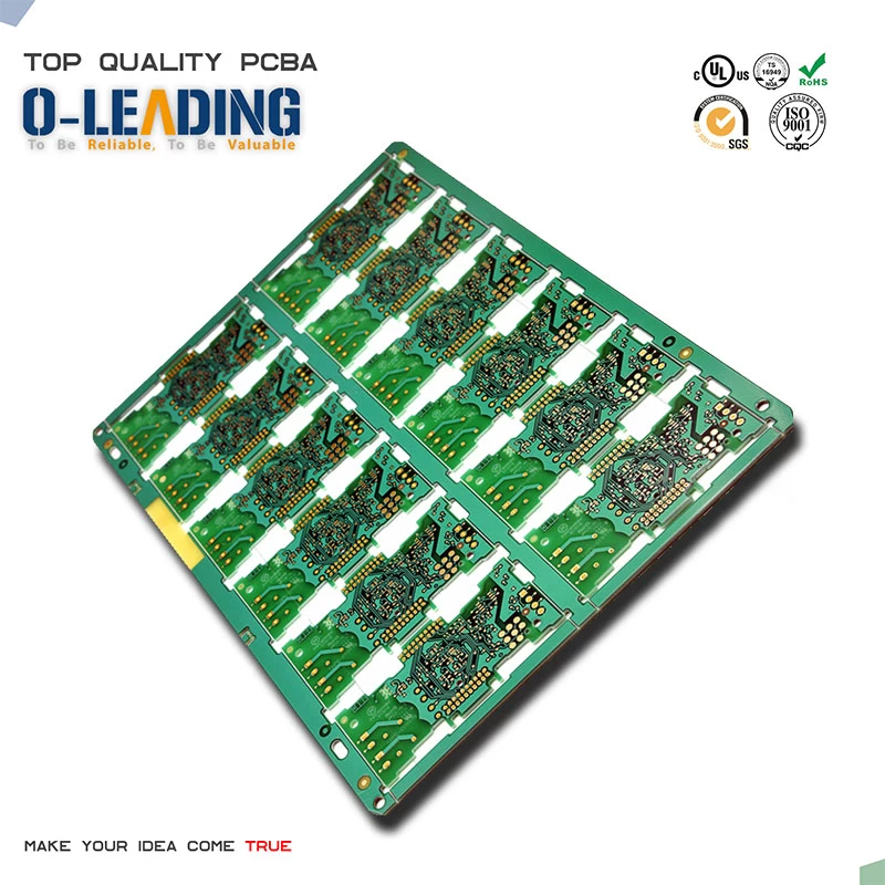
China Electronic Circuit Board PCB Assembly Board customized SMT PCBA fabricatio Printed Circuit Board
- Model Number:1684I0088
- Place of Origin:Guangdong, China
- Product name:Printed Circuit Board
- Type:Electroplated Gold + Gold Finger
- Usage:OEM Electronics
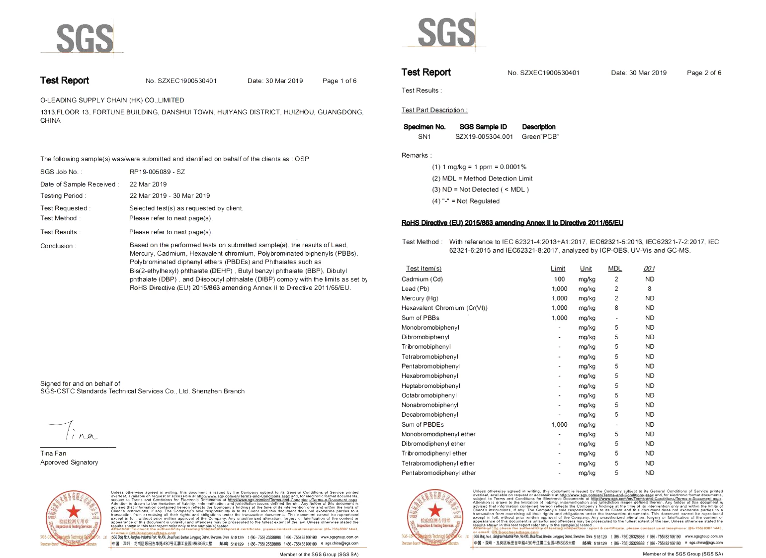
- Certificate:ROSH. ISO9001
- Solder mask:Green. Red. Blue. White. Black.Yellow
- Material:FR4 /aluminum/ceramic CEM1
- Service:One Stop Turkey Service
- Function:Control Key Board PCB
- PCB Standard:IPC-A-600
- Brand Name:O-leading
- Base Material:FR-4/CEM-1/CEM-3/Polyimild/PTFE/Rogers
- Copper Thickness:0.4-2mil(10-50um)
- Board Thickness:0.2-6mm
| Welcome to O-leading |
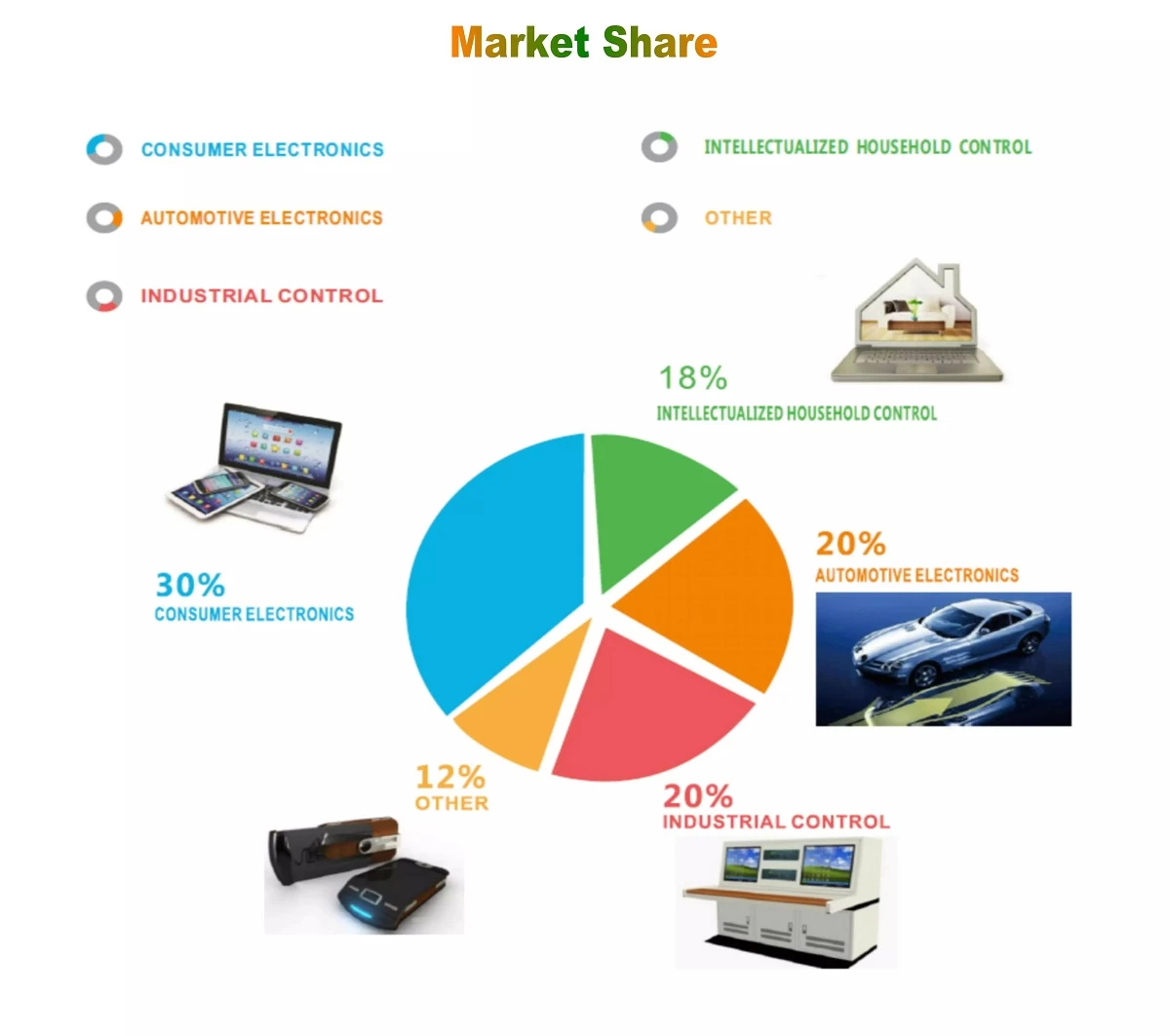
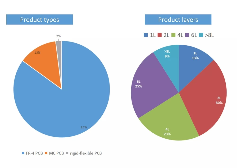
O-Leading China PCB Assembly PCBA Manufacturer strives to be your one stop solution partner in EMS supply chain, including PCB design , PCB fabrication and PCB assembly,We provide some of the most advanced PCB technology, including HDI PCBs,multilayer PCBs, Rigid-Flexible PCBs.We can support from quick turn prototype to medium & mass Production.
In general, our global customers are very impressed with our services:Rapid response, competitive price and quality commitment.Providing more valuable technical service and overall solution is the way O-leading forward.
Looking to the future, O-leading will concentrate on the innovation and development of electronics manufacturing technology as always, and make persistent efforts on PCB & PCBA one-stop service to provide first-class services and create more value for our customers.
PLEASE CLICK THESE FOR MORE INFORMATION:OEM PCBA Assembling Protective PCB Coating Board


| Product Description |
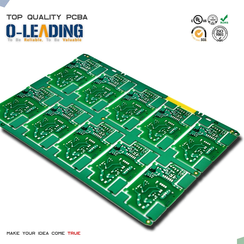
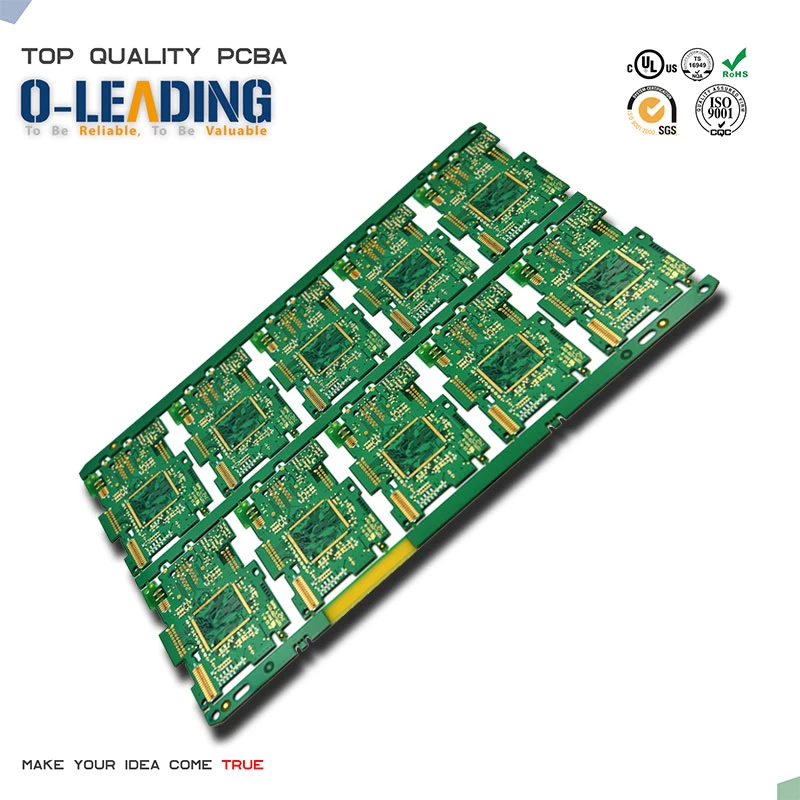
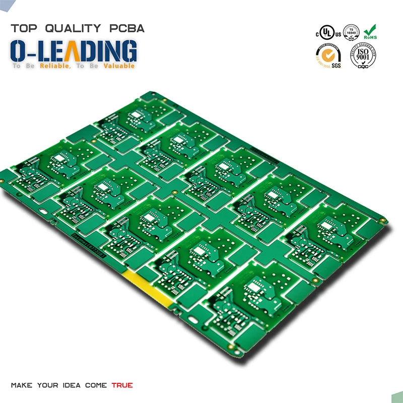
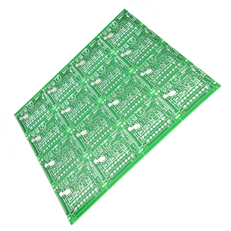
China Electronics Multilayer and Double-Sided PCB,Electronic Circuit Board PCB Assembly Board customized SMT PCBA fabricatio Printed Circuit Board
| Product name | Printed Circuit Board |
| Brand Name | O-leading |
| Base Material | FR-4/CEM-1/CEM-3/Polyimild/PTFE/Rogers |
| Copper Thickness | 0.4-2mil(10-50um) |
| Board Thickness | 0.2-6mm |
| Min. Hole Size | 0.1mm(4mil)for HDI / 0.15mm(6mil) |
| Min. Line Width | 0.075mm/0.075mm(3mil/3mil) |
| Min. Line Spacing | 0.003'' |
| Surface Finishing | HASL/OSP/Ag/ENIG/ENEPIG/Immersion silver,Tin |


| Our Team |
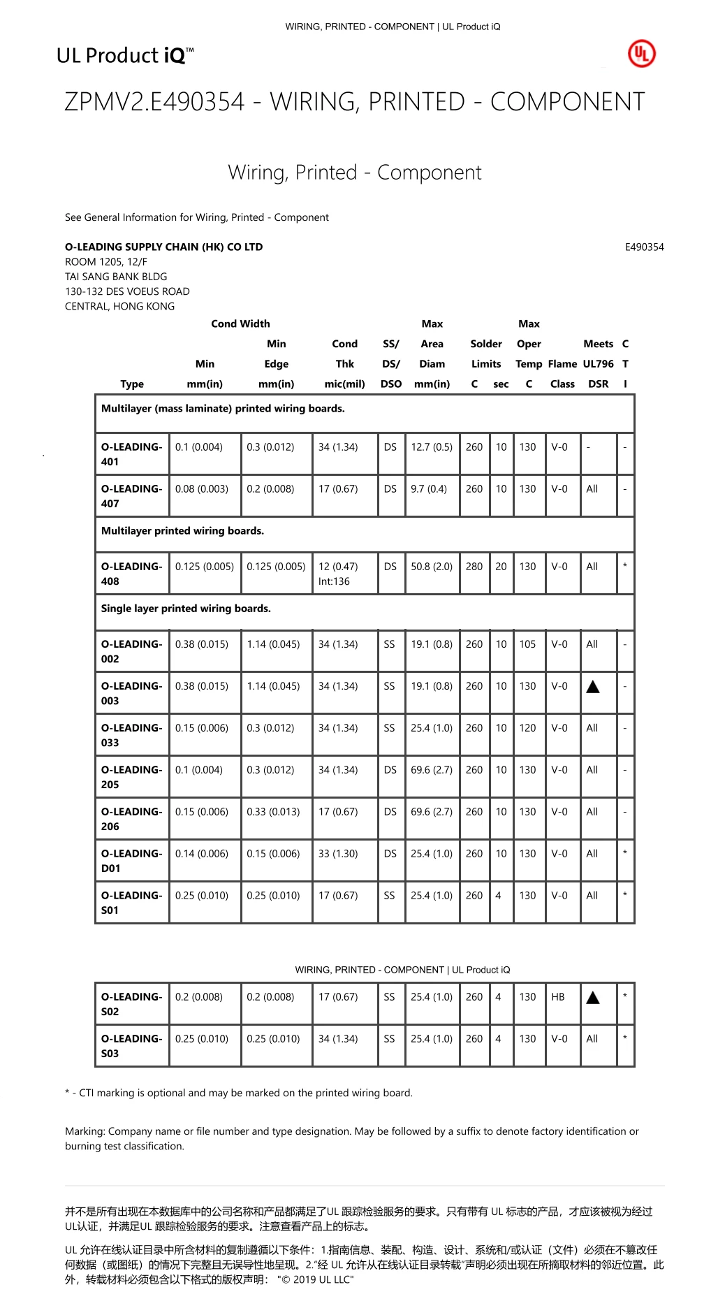
| Certifications |
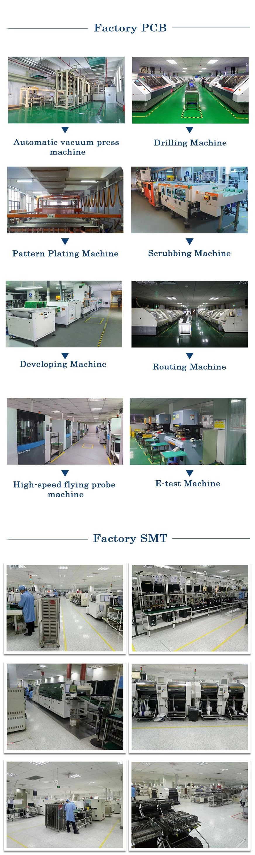
| Process Capability |
| PCB Production Capabilities | |
| Layer Count | 1Layer-32Layer |
| Finished copper thickness | 1/3oz-12oz |
| Min Line width/spacing internal | 3.0mil/3.0mil |
| Min Line width/spacing external |
4.0mil/4.0mil |
| Max Aspect Ratio | 10:1 |
| Board thickness | 0.2mm-5.0mm |
| Max Panel size(inches) | 635*1500mm |
| Minimum Drilled Hole Size | 4mil |
| PIated Hole Tolerance | +/-3mil |
| BIind/Buried Vias (AII Types) | YES |
| Via Fill(Conductive,Non-Conductive) | YES |
| Base Material | FR-4,FR-4high Tg.Halogen free material,Rogers,Aluminium base,Polyimide,Heavy Copper |
| Surface finishes | HASL,OSP,ENIG,HAL-LF,lmmersion silver,lmmersion Tin,Gold fingers,Carbon ink |
| SMT Production Capabilities | |
| PCB Material | FR-4,CEM-1,CEM-3,Aluminum-based board,FPC |
| Max PCB size | 510x1500mm |
| Min PCB size | 50x50mm |
| PCB Thickness | 0.5mm-4.5mm |
| Board thickness | 0.5-4mm |
| Min Components size | 0201 |
| Standard chip size component |
0603 and larger |
| Component max height | 15mm |
| Min lead pitch | 0.3mm |
| Min BGA ball pitch | 0.4mm |
| Placement precision | +/-0.03mm |
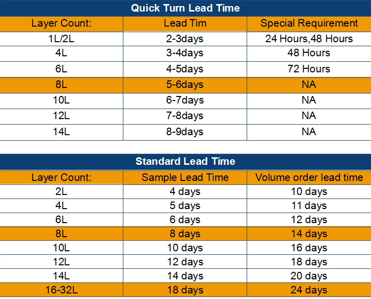
| Packaging & Delivery |

| FAQ |
1.1 The process is strictly controlled under ISO 9001:2008 standards.
1.2 Extensive use of software in managing the production process
1.3 State-of-art testing equipments and tools. E.g. Flying Probe, X-ray Inspection, AOI (Automated Optical Inspector) and ICT(in-circuit testing).
1.4.Dedicated quality assurance team with failure case analysis process
1.5.Continuous staff training and education
2. How do O-Leading keep your price competitive?
Over the last decade, prices of many raw materials (e.g. copper, chemicals) had doubled, tripled or quadrupled; Chinese currency RMB had appreciated 31% over US dollar; And our labor cost also increased significantly.
However, O-Leading have kept our pricing steady. This owns entirely to our innovations in reducing cost, avoiding wastes and improving efficiency. Our prices are very competitive in the industry at the same quality level.
We believe in a win-win partnership with our customers. Our partnership will be mutually beneficial if we can provide you anedgeon cost and quality.
3. What kinds of boards can O-Leading process?
Common FR4, high-TG and halogen-free boards, Rogers, Arlon, Telfon, aluminum/copper-based boards, PI, etc.
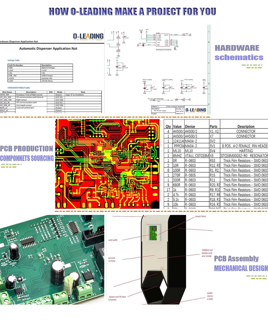
4. What data are needed for PCB & PCBA production?
4.1 BOM (Bill of Materials) with reference designators: component description, manufacturer’s name and part number.
4.2 PCB Gerber files.
4.3 PCB fabrication drawing and PCBA assembly drawing.
4.4 Test procedures.
4.5 Any mechanical restrictions such as assembly height requirements.
5. What’s the typical process flow for multi-layer PCB?
Material cutting → Inner dry film → inner etching → Inner AOI → Multi-bond→ Layer stack up Pressing → Drilling → PTH → Panel Plating → Outer Dry Film → Pattern Plating → Outer etching → Outer AOI → Solder Mask → Component Mark → Surface finish → Routing → E/T → Visual Inspection.
6. What’s the key equipments for HDI manufacturing?
Key equipment list is as following: Laser drilling machine, Pressing machine, VCP line, Automatic Exposing machine, LDI and etc. The equipments we have are the best in the industry, laser drilling machines are from Mitsubishi and Hitachi, LDI machines are from Screen(Japan), Automatic Exposing machines are also from Hitachi, all of them make we can meet customer’s technical requirements.
7. How many types of surface finish O-lead can do?
O-the leader has the full series of surface finish, such as: ENIG, OSP, LF-HASL, gold plating (soft/hard), immersion silver, Tin, silver plating, immersion tin plating, carbon ink and etc. .. OSP, ENIG, OSP + ENIG commonly used on the HDI, we usually recommend that you use a client or OSP OSP + ENIG if BGA PAD size less than 0.3 mm.
8. What’s your capability for FPC? Can O-Leading provide SMT service also?
O-Leading can fabricate FPC from single layer to 8layer, the working panel size can be as large as 2000mm*240mm, please find the details in the page “Flex Capability”. We also provide SMT one stop service to customer.
9. What are the main factors which will affect the price of PCB?
Material;
Surface finish;
Technology difficulty;
Different quality criteria;
PCB characteristics;
Payment terms;
Different manufacturing countries.
10. What’s the definition of PCB, PWB and FPC and what’s the difference?
PCB is short for Printed Circuit Board;
PWB is short for Printed Wire Board, same meaning as Printed Circuit Board;
FPC is short for Flexible Printed Board.
11. What factors should be considered when choosing the material for a PCB board?
Below factors should be considered when we choose the material for PCB:
The material’s Tg value should be greater than the operation temperature;
Low CTE material has good performance of thermal stability;
Good thermal resistance performance: Normally PCBs are required to resist 250℃ for at least 50s.
Good flatness; In consideration of the electrical properties, low loss/high permittivity material is used on high frequency PCB;
Polyimide glass fiber substrate used for flexible PCB; Metal core is used when the product has strict requirement of heat
dissipation.
12. What’s the merits of O-leading's rIgid-flex PCB?
O-leading’s rigid-flex PCB has the characters of both FPC and PCB, so it can be used in some special products. Some part is flexible while the other part rigid, it can help save product’s interior space, reduce product volume and improve performance.
13. How to you make the impedance calculation?
The impedance control system is done using some test coupons, the SI6000 soft and the CITS 500s equipment from POLAR INSTRUMENTS. The equipment measures the impedance on a representative track configuration coupon of which the client has given us a determinate value and tolerance.
- Other Products


