


- Contact Us
-
TEL: + 86-13428967267
FAX: + 86-4008892163-239121
+ 86-2028819702-239121
Email: sales@o-leading.com Contact Now
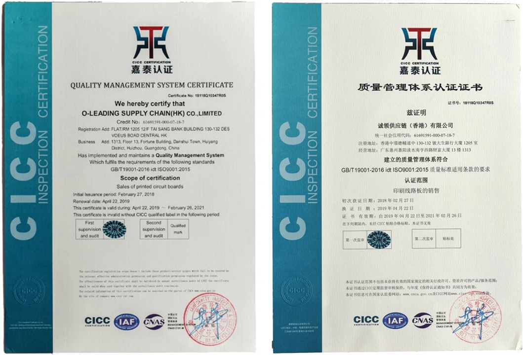
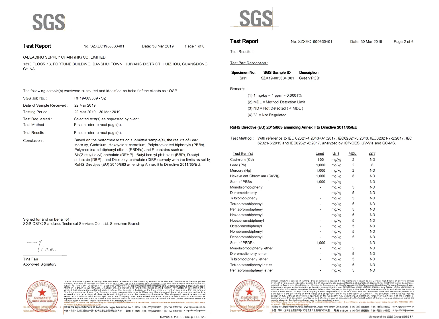
- Certifications
-


- Subscribe
-
Get email updates on new products
- New Products


- Electronic album


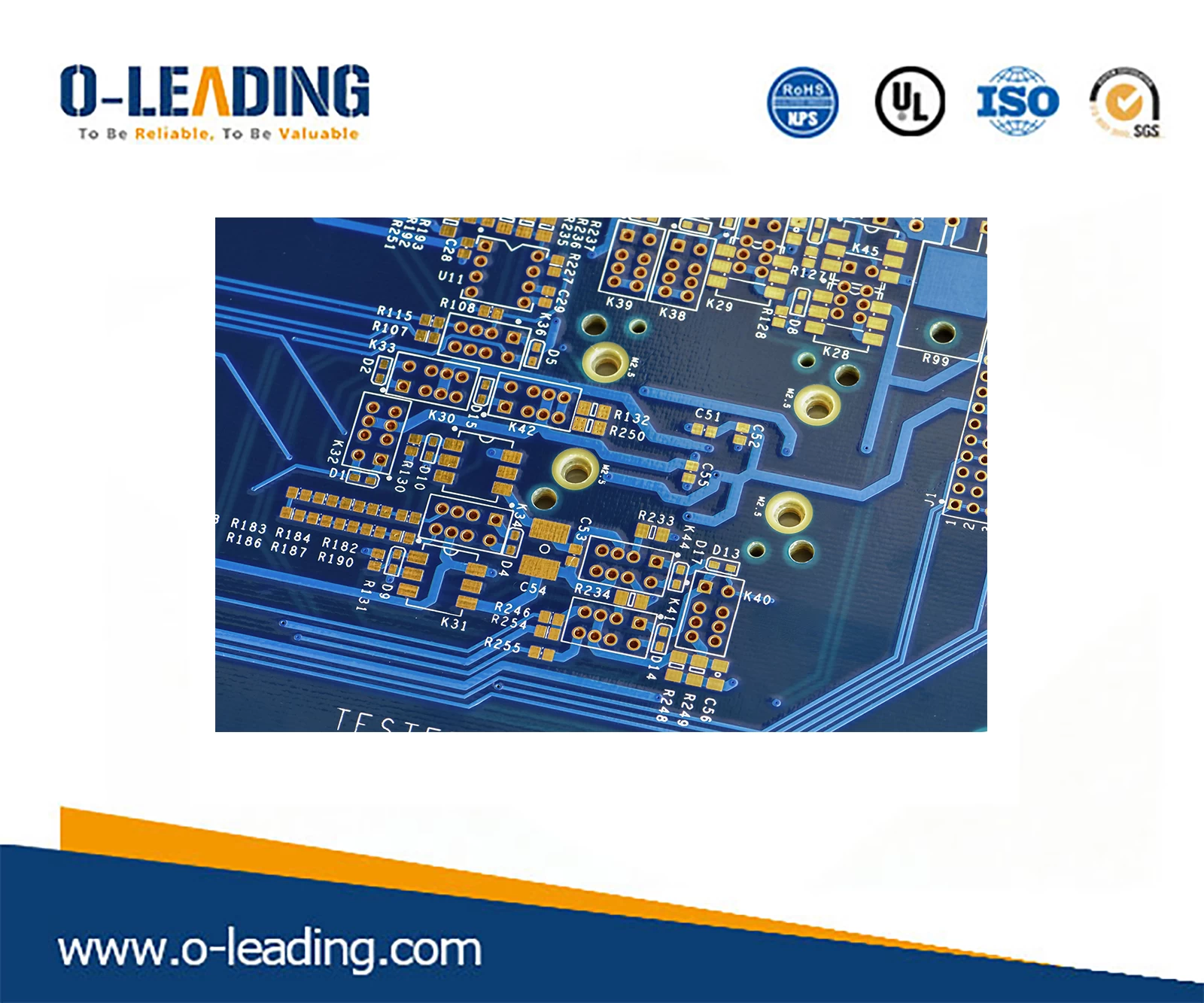
Multilayer board manufacturer china, Prototype PCB Assembly company china
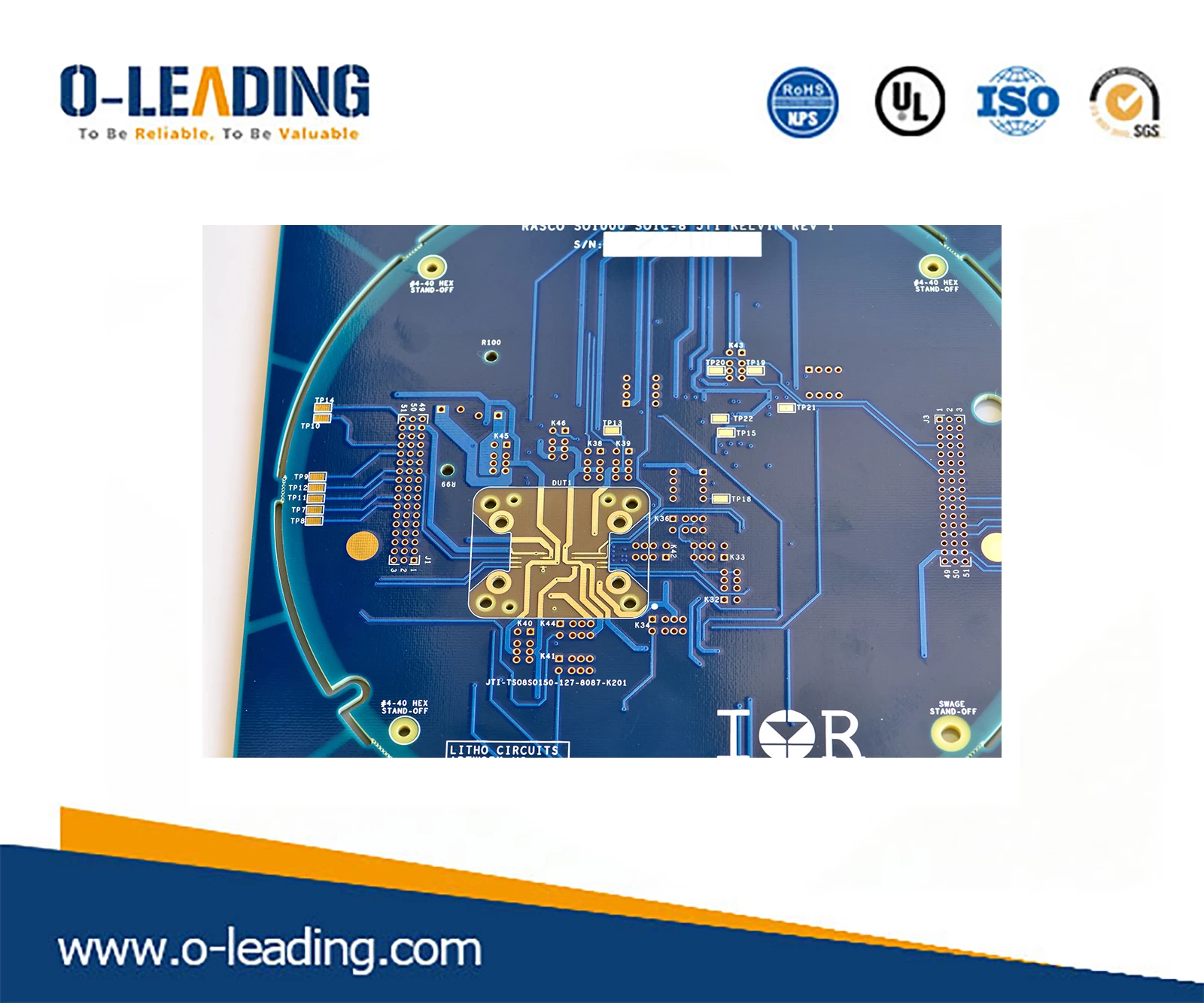
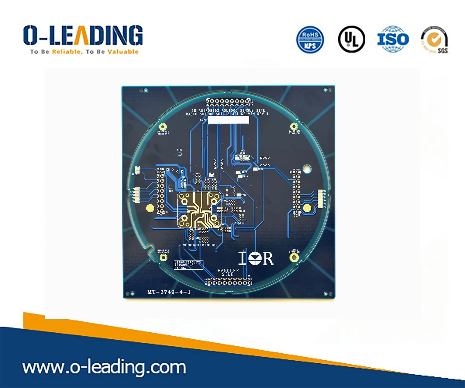
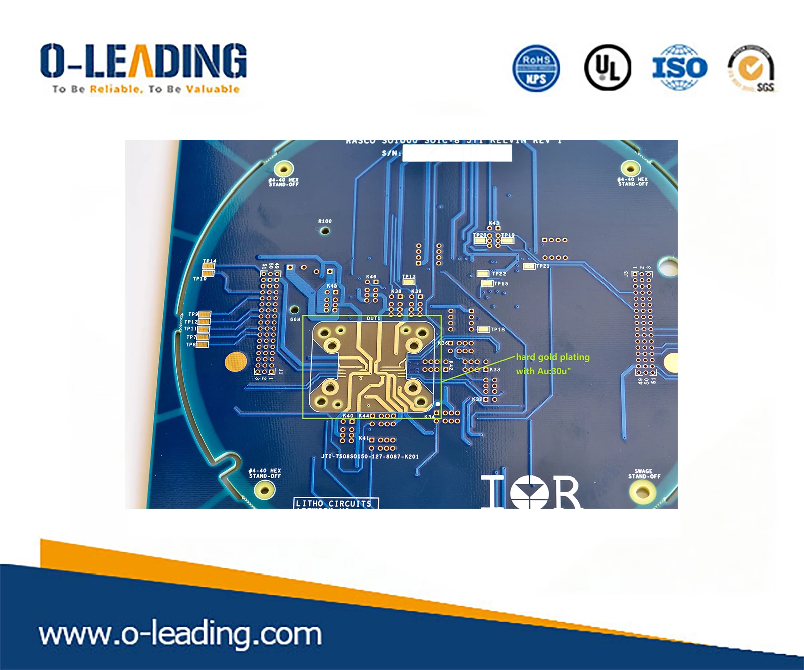
- PCB P/N: D1868A
- Layer Count:4L HDI
- Material:FR-4 TG150
- Board thk:3.175mm
- copper thk:2/2/2/2oz
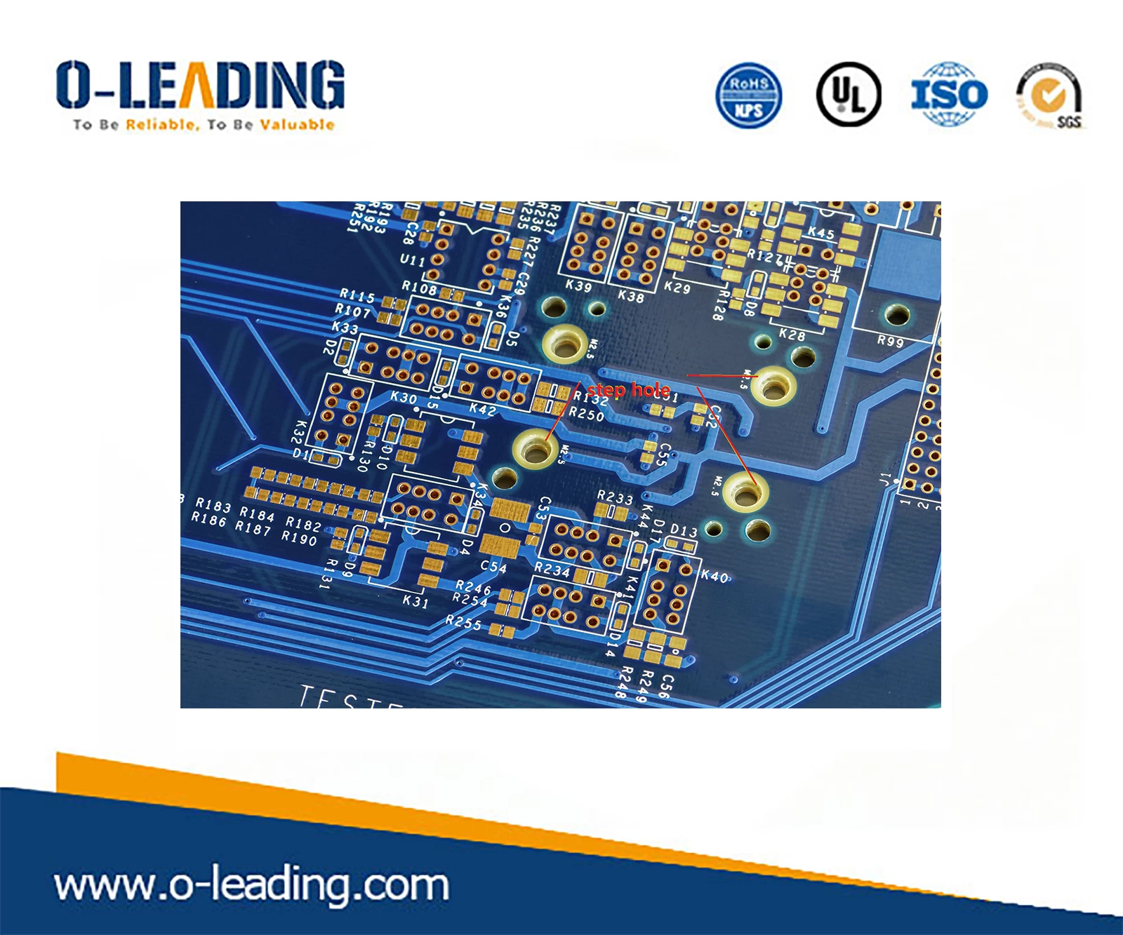
- Smallest hole size:0.3MM
- No. of holes (pcs):471
- line w/s:12/12mil
| Welcome to O-leading |
O-Leading strives to be your one stop solution partner in EMS supply chain, including PCB design , PCB fabrication and PCB assembly (PCBA).We provide some of the most advanced PCB technology, including HDI PCBs,multilayer PCBs, Rigid-Flexible PCBs.We can support from quick turn prototype to medium & mass Production. (Multilayer PCB manufacturer china)
In general, our global customers are very impressed with our services:rapid response, competitive price and quality commitment.Providing more valuable technical service and overall solution is the way O-leading forward.
Looking to the future, O-leading will concentrate on the innovation and development of electronics manufacturing technology as always, and make persistent efforts on PCB & PCBA one-stop service to provide first-class services and create more value for our customers.
| Product Description |
| PCB P/N | D1868A |
| Layer Count | 4L HDI |
| Material | FR-4 TG150 |
| Board thk | 3.175mm |
| copper thk | 2/2/2/2oz |
| Smallest hole size | 0.3MM |
| No. of holes (pcs) | 471 |
| line w/s | 12/12mil |
| Impedance control. Y / N (Tol %) | Y |
| Surface Finishing:Plated hard Gold, Au | 1.27um min |
| Solder Mask Silkscreen | Blue / White |
| Single board size | Dim X (mm): 203.20;Dim Y (mm): 203.20 |
| Panelisation | Dim X (mm): 217.2;Dim Y (mm): 217.2;No Of UPS:1 |
| Special:peelable mask | N |
| Routing/Punching | CNC |


| Our Team |

| Certifications |
| Packaging & Delivery |

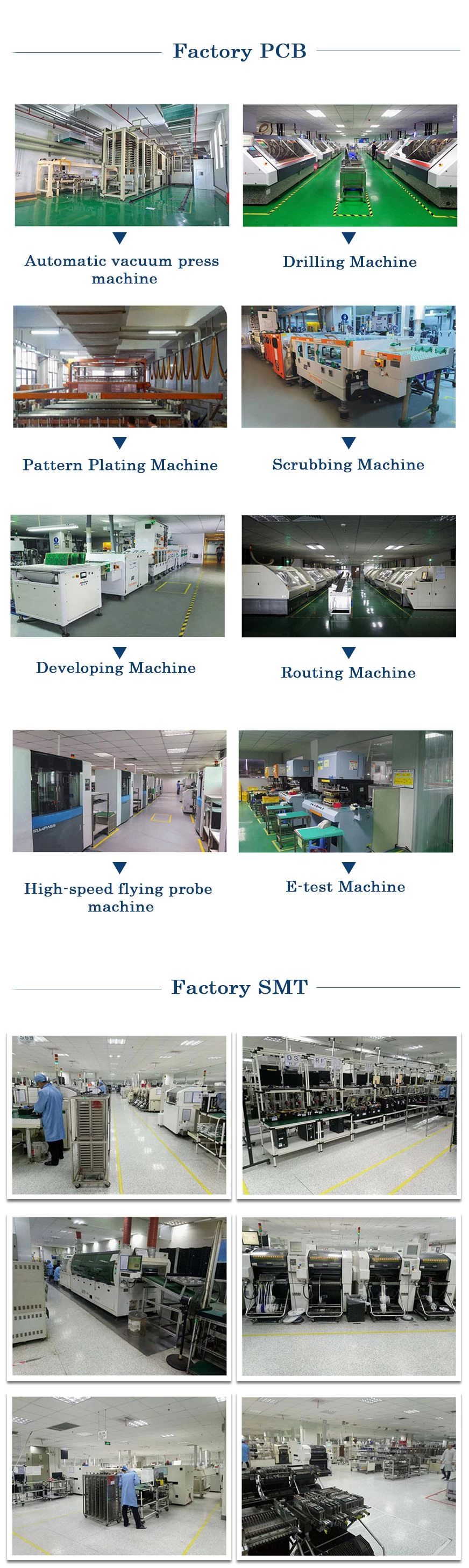
| Process Capability |
PCB Production Capabilities
Layer Count: 1Layer-32Layer
Finished copper thickness: 1/3oz-12oz
Min Line width/spacing internal: 3.0mil/3.0mil
Min Line width/spacing external: 4.0mil/4.0mil
Max Aspect Ratio: 10:1
Board thickness: 0.2mm-5.0mm
Max Panel size(inches): 635*1500mm
Minimum Drilled Hole Size: 4mil
PIated Hole Tolerance: +/-3mil
BIind/Buried Vias (AII Types): YES
Via Fill(Conductive,Non-Conductive): YES
Base Material: FR-4,FR-4high Tg.Halogen free material,Rogers,Aluminium base,Polyimide,
Heavy Copper
Surface finishes: HASL,OSP,ENIG,HAL-LF,lmmersion silver,lmmersion Tin,Gold fingers,Carbon ink
SMT Production Capabilities
PCB Material: FR-4,CEM-1,CEM-3,Aluminum-based board
Max PCB size: 510x460mm
Min PCB size:50x50mm
PCB Thickness:0.5mm-4.5mm
Board thickness:0.5-4mm
Min Components size: 0201
Standard chip size component: 0603 and larger
Component max height:15mm
Min lead pitch: 0.3mm
Min BGA ball pitch:0.4mm
Placement precision: +/-0.03mm
- Other Products


