


PCBA shielding mold wave soldering process technology
1.Advantages of using shielded mold wave soldering technology
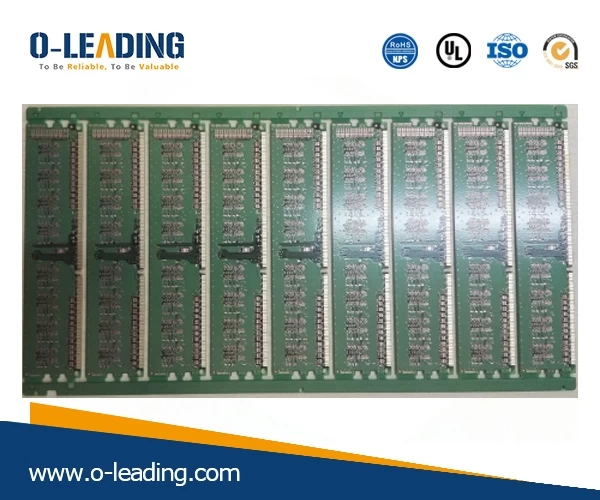
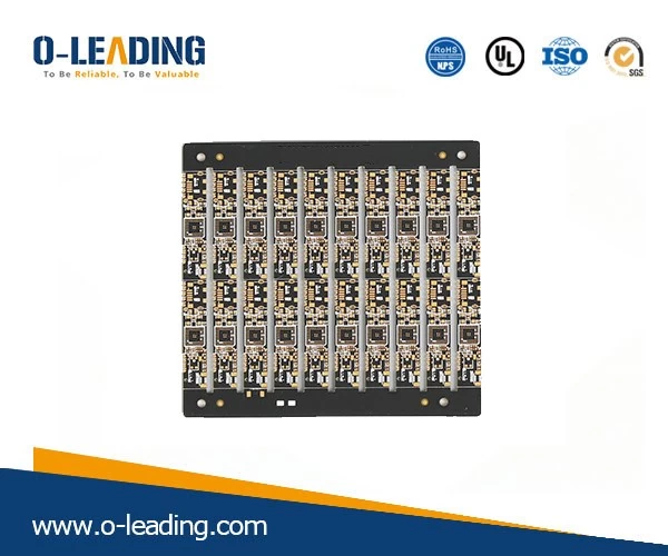
1) The realization of double-sided mixed PCB wave soldering production can greatly improve the production efficiency of double-sided mixed PCB and avoid the problem of poor quality consistency in manual soldering.
2) Reduce the preparation time for solder resist, improve production efficiency, and reduce production costs.
3) The output is equivalent to traditional wave soldering.
Blind-buried board supplier china
2.Shield mold material
1) The mold must be anti-static. Common materials are: aluminum alloy, synthetic stone, fiberboard. In order to avoid the wave soldering sensor being insensitive when using synthetic stones, it is recommended not to use black synthetic stones.
2) Make the mold substrate thickness. According to the thickness of the components on the back of the machine disk, a substrate with a thickness of 5mm to 8mm is selected to make a mold.
3. Mold process size requirements
1) Overall dimensions of the mold: The length and width of the mold are equal to the length and width of the PCB plus the width of the side of the carrier of 60mm, and the mold width must be ≦ 350mm. When the PCB width is less than 140mm, you can consider placing two PCBs for soldering in one mold at the same time.
2) The process edge is 8mm away from the edge, and the other two sides are close to the edge to install a 10mm wide and 10mm high bakelite strip to increase the strength of the mold and reduce mold deformation.
3) Each reinforcement bar must be fixed with screws, and the distance between the screws and the screws is below 150mm.
4) After the mold is made, press buckles (fixing the PCB on the mold) must be installed within a distance of 100mm around the mold, and the following points must be noted:
① Do not touch the parts after one rotation;
② Does not affect DIP plug-ins;
③ PCB can be firmly fixed in the mold.
5) The four corners of the mold should be chamfered with R5.
6) When the PCBA on the mold passes through the tin furnace, some parts will be floated by the impact of tin waves. Therefore, some parts that are easy to float high will be pressed to solve the problem.
The main methods currently used:
① Metal iron block pressing pieces;
② Install crimping parts on the mold;
③ Make anti-floating high-pressure parts fixture.