


PCB failure analysis technology (3)
Photoelectron spectroscopy (XPS) analysis
When the sample is irradiated with X-rays, the inner shell electrons of the surface atoms will escape from the bondage of the atomic nucleus and escape from the solid surface to form electrons. The kinetic energy of the electrons can be measured by Ex. Different electron shells are different, it is the "fingerprint" identification parameter of the atom, and the formed spectral line is the photoelectron spectroscopy (XPS). XPS can be used for qualitative and quantitative analysis of shallow surface (several nanometers) elements on the sample surface. In addition, information about the chemical valence of an element can be obtained based on the chemical shift of the binding energy. It can give information such as the atomic valence of the surface layer and surrounding elements; the incident beam is an X-ray photon beam, so it can analyze the insulating sample without damaging the analyzed sample, and fast multi-element analysis can be performed; also under the condition of argon ion peel The longitudinal element distribution analysis is performed on multiple layers, and the sensitivity is much higher than that of energy spectrum (EDS). In the analysis of PCB, XPS is mainly used for the analysis of the quality of the pad coating, the analysis of the contamination, and the analysis of the degree of oxidation to determine the deep-seated cause of poor solderability.
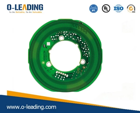
Automobile Navigation Immersion Gold PCB
Thermal Analysis Differential Scanning Calorim-etry
A method of measuring the relationship between the power difference between the input material and a reference material as a function of temperature (or time) under programmed temperature control. DSC is equipped with two sets of compensation heating wires under the sample and reference container. When the temperature difference ΔT between the sample and the reference occurs due to the thermal effect during the heating of the sample, the differential thermal amplification circuit and differential thermal compensation amplifier can be used. , So that the current flowing into the compensation heating wire changes.
And make the heat balance on both sides, the temperature difference ΔT disappears, and record the relationship between the thermal power difference between the two electrothermal compensations under the sample and the reference as a function of temperature (or time). Chemical and thermodynamic properties. DSC is widely used, but in the analysis of PCB, it is mainly used to measure the curing degree and glass transition temperature of various polymer materials used on the PCB. These two parameters determine the reliability of the PCB in the subsequent process.
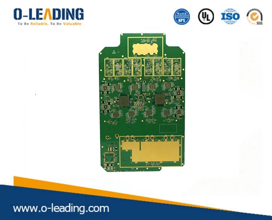
Power supply module manufacturer china
Thermomechanical Analyzer (TMA)
Thermal Mechanical Analysis technology is used to measure the deformation properties of solids, liquids and gels under the action of heat or mechanical force under temperature control. Common load methods are compression, needle penetration, stretching, bending, etc. The test probe is supported by a cantilever beam and a coil spring fixed on it. A load is applied to the sample by the motor. When the sample deforms, the differential transformer detects this change and processes it with temperature, stress and strain data. The relationship between the deformation of a substance under a negligible load and temperature (or time) can be obtained. According to the relationship between deformation and temperature (or time), physical and chemical and thermodynamic properties of materials can be studied and analyzed. TMA is widely used. In the analysis of PCB, it is mainly used for the two most critical parameters of the PCB: measuring its linear expansion coefficient and glass transition temperature. PCBs with substrates with excessive expansion coefficients often lead to failure of metallized holes after solder assembly.
Due to the development trend of high-density PCBs and environmental protection requirements of lead-free and halogen-free, more and more PCBs have encountered various failure problems such as poor wetting, bursting, delamination, and CAF. The application of these analysis techniques in practical cases is introduced. Obtaining the failure mechanism and cause of PCB will be beneficial to the quality control of PCB in the future, so as to avoid similar problems from happening again.