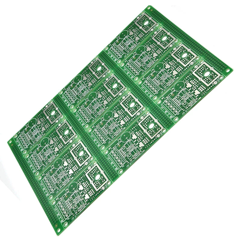
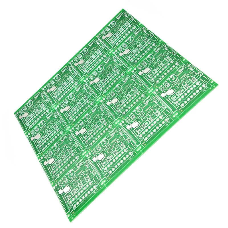
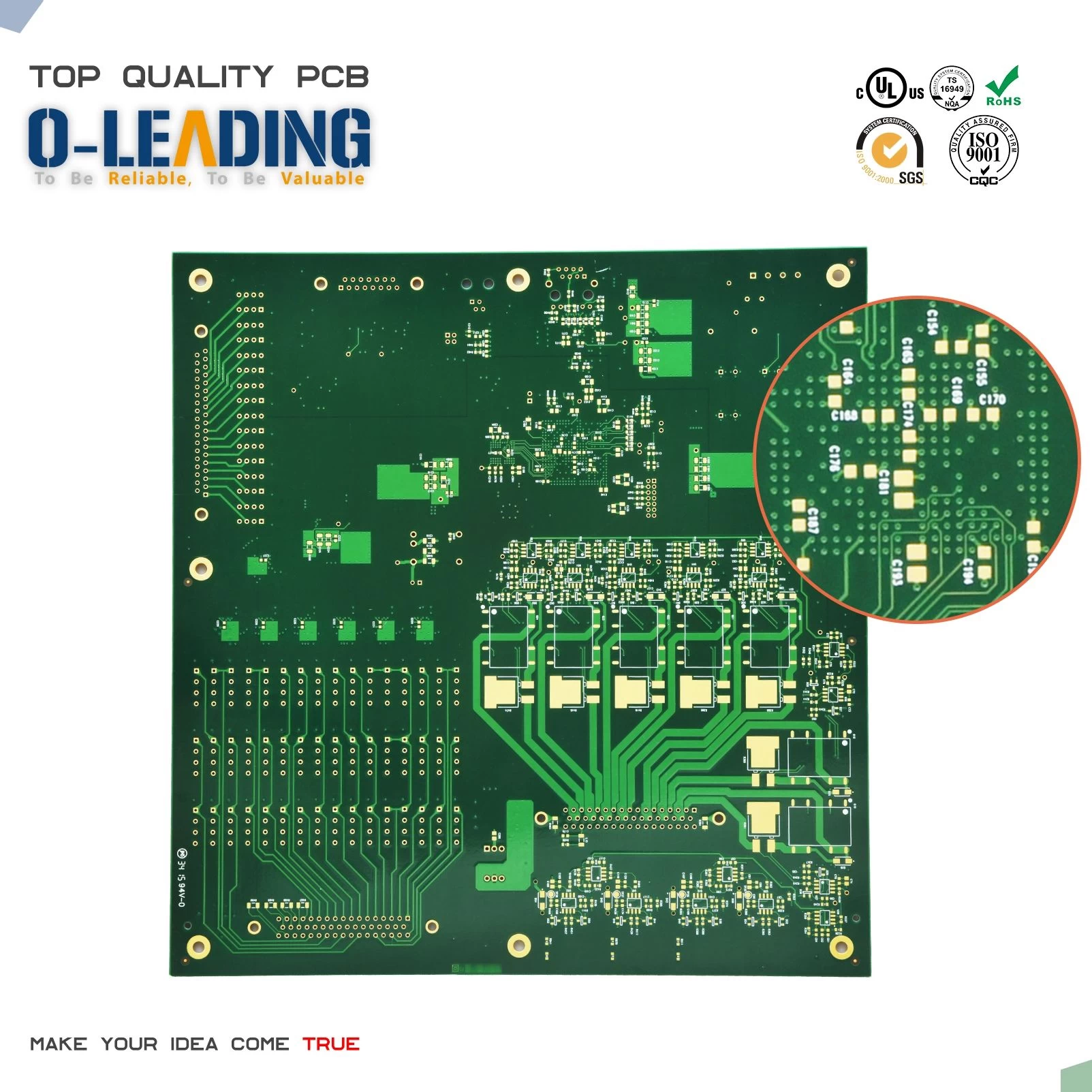
Is the bottom layer copper good for PCB?
In the process of PCB design, some engineers do not want to lay copper on the entire surface of the bottom layer in order to save time. Is this right? Is it necessary for the PCB to be copper-plated?
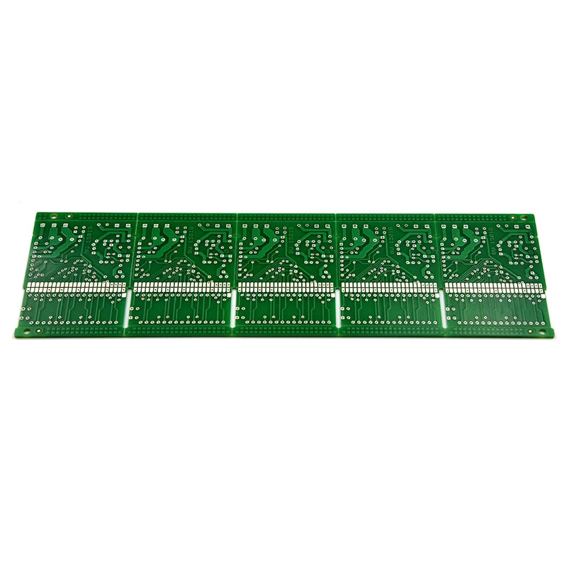
First of all, we need to be clear: copper plating on the bottom layer is beneficial and necessary for the PCB, but copper plating on the entire board must comply with certain conditions.
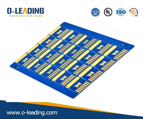
Benefits of copper plating on the bottom layer of the table
1. From the perspective of EMC, the entire surface of the bottom layer is covered with copper, which provides additional shielding protection and noise suppression for the inner layer signal and the inner layer signal. At the same time, it also has certain shielding protection for the bottom layer device and signal.
2. From the perspective of heat dissipation, due to the increasing density of current PCB boards, BGA main chips also need to consider thermal issues more and more. The whole board is grounded with copper to improve the heat dissipation ability of the PCB.
3. From the perspective of the process, the entire board is grounded with copper to make the PCB board evenly distributed. PCB bending and board warping are avoided during PCB processing and pressing. At the same time, the stress caused by PCB reflow soldering due to uneven copper foil is not caused. The PCB is warped.
Reminder: For two-layer boards, copper clad is necessary
On the one hand, because the two-layer board does not have a complete reference plane, paving the ground can provide a return path and can also be used as a coplanar reference to achieve the purpose of controlling impedance. We can generally lay the ground plane on the bottom layer, and put the main components and power lines and signal lines on the top layer. For high-impedance circuits, analog circuits (analog-to-digital conversion circuits, switch-mode power conversion circuits), copper clad is a good practice.
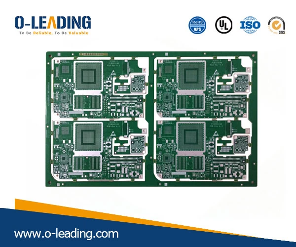
Conditions for copper plating on the bottom surface
Although the bottom layer of copper is good for PCB, there are some conditions that need to be followed:
1. Lay as much as possible at the same time, do not cover it all at once, avoid broken copper skin, and add vias to the ground plane in the copper area.
Reason: The copper-clad plane on the surface layer must be fragmented and broken by the components and signal wires on the surface layer. If there is poorly grounded copper foil (especially the thin and long broken copper), it will become an antenna and cause EMI problems. .
2. Consider the thermal balance of small packages, especially small packages such as 0402 0603, to avoid the monument effect.
Reason: If the entire board is copper-plated, the copper of the component pins will be fully connected with copper, which will cause the heat to be dissipated too quickly, which will cause difficulties in desoldering and rework soldering.

3. The grounding of the entire board is preferably continuous grounding. The distance from the grounding to the signal needs to be controlled to avoid discontinuities in the transmission line impedance.
Reason: Copper sheets that are too close to the ground will change the impedance of the microstrip transmission line, and discontinuous copper sheets will also have a negative impact on the impedance discontinuities of the transmission line.
4. Some special situations depend on the application scenario. PCB design should not be an absolute design, and it should be weighed and used in combination with various theories.
Reason: In addition to the sensitive signal that needs to be grounded, if there are many high-speed signal lines and components, a lot of small and long broken copper is generated, and the wiring channels are tight, it is necessary to avoid surface copper holes to connect to the ground plane as much as possible. The surface layer can choose not to be copper.

