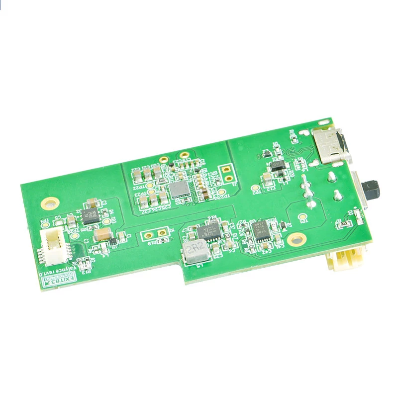
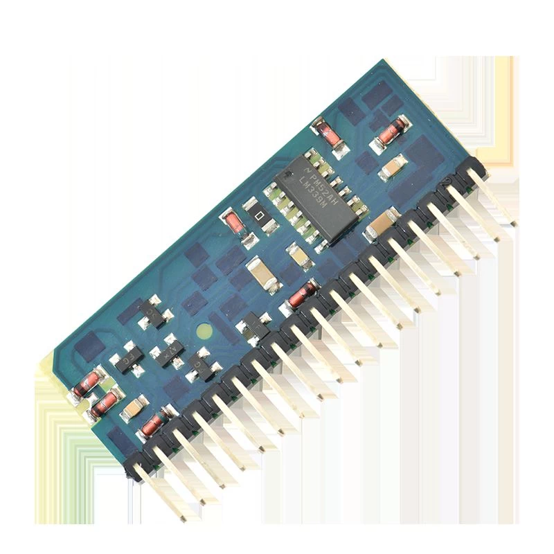
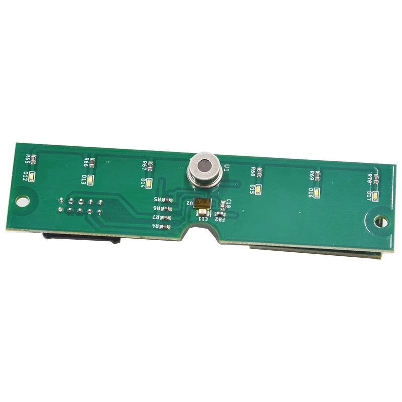
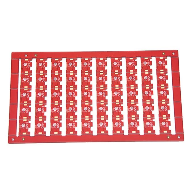
The "5 kinds" production process that must be considered before the pcb layout
First, is the single or double board?
Second, is it all in-line or in-line plus patch?
Third, does the factory support the red glue process?
Converting into practical problems is a mainstream design and production solution. 3D printer PCB supplier.
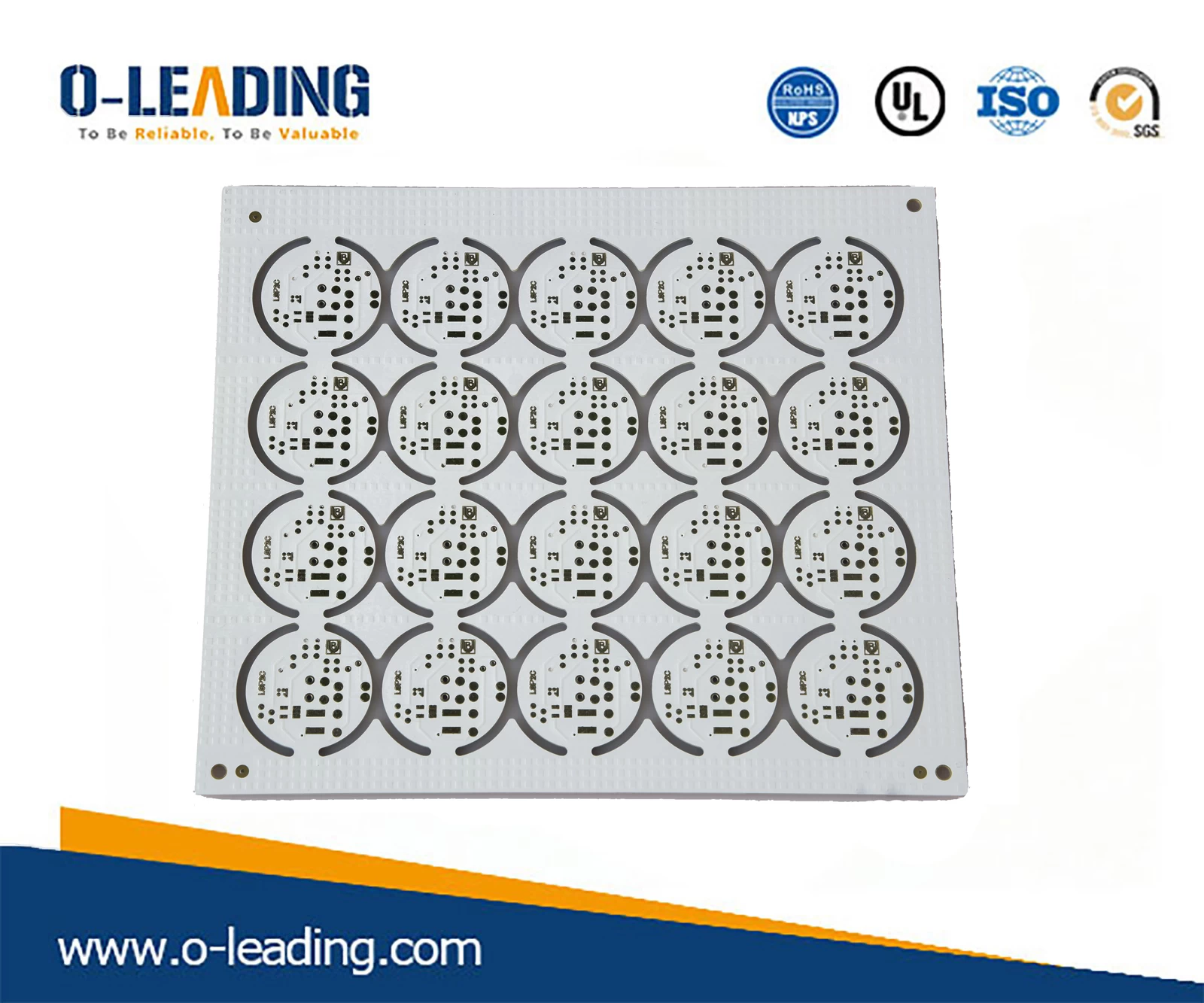
Option One
Full straight plug, single panel
Program 1 cost analysis
---Hand plug, once wave soldering
The earliest power supplies were designed this way. After all, wave soldering and reflow soldering were not popular at the time. The most traditional tin pots used by people. (exposure age)
A design note log for a switching power supply engineer, part 5 costing and summarizing
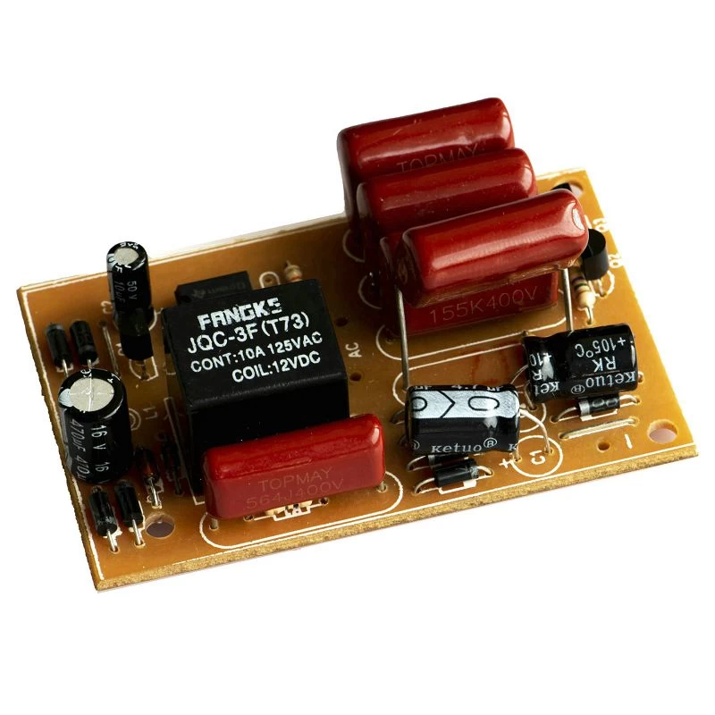
The full plug-in + single-sided paper PCB version is almost an era of the past era, and it has been used very little now.
Printed circuit boards supplier.
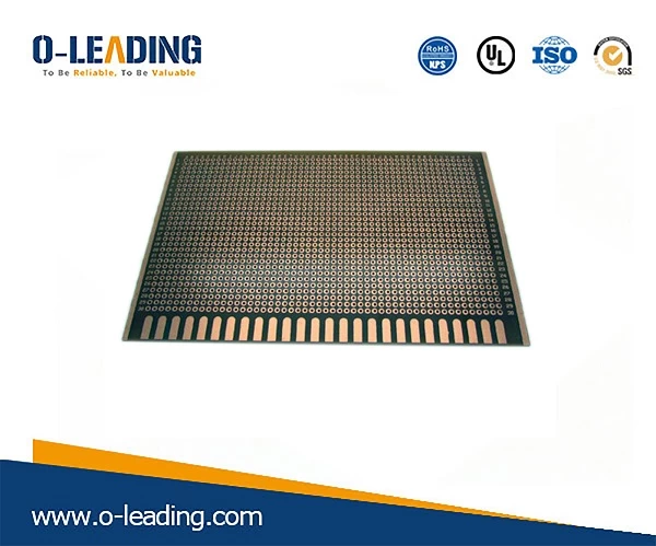
Option II
Patch + plugin, patch and plugin one side.
Option 2 cost analysis
---Reflow soldering once, once again wave soldering
A reflow soldering + a wave soldering is actually a standard for many companies' production lines, so the power supply designed by this solution is also the easiest product to be produced.
third solution
Patch + plug-in, patch on the bottom, plug-in on the top
Option 3 cost analysis
--- First reflow soldering, soldering chip components. Then make a fixture to block the patch components. Finally, visit the connectors and cross the wave soldering.
The cost is this
Wave soldering + reflow + fixture cost
In the picture is the so-called jig, through a special baffle, the patch components are blocked, only the pins of the straight insert are exposed, and then the wave soldering can be performed. However, the precondition is that the distance between the chip component and the straight card is far enough, and the cost of the jig is not low.
AOI Testing supplier china.
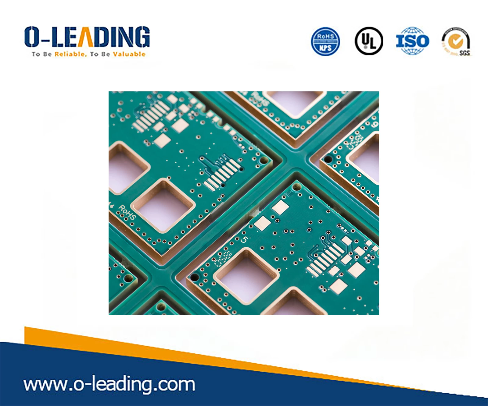
However, in reality, due to the compact size requirements of modern power supplies, it is impossible to leave sufficient fixture isolation space for the components of the chip components and the in-line components. So the common practice is to glue the chip components to the reverse side of the circuit board through the red glue, then place the plug-in, and finally unify the wave soldering.
The cost is this
Red plastic cost + wave soldering
The reason for this is because it is cheap. Of course, the prerequisite is that your factory has such a device as a red glue machine.
Option 3 is also the most common production solution for modern power production. Of course, for example, our company does not have a red glue machine, so I chose the second option, which is reflow + one wave soldering, and the second is relative to the third, because the chip components and the inline components are on one mounting surface. Therefore, it will occupy a special area of the PCB, which indirectly imposes requirements on the layout capability of the power supply engineer.
PS: Option 3 has a more deductible approach, which is to make a single panel. Everything else remains the same. The advantage is that you can save a little price on the PCB. But the downside is that wiring is more difficult.
The PCB that we analyzed before is doing this. Of course, everyone should also notice that this board needs a flying line. The flying line is actually a custom piece, and it is not convenient to use the machine to plug in, so it is recommended that you use it directly. The double panel is all right. After all, the cost of dual-panel is not much higher now.
Option four
Two-sided patch + straight plug
Option 4 is definitely a local tyrant. Design that doesn't care about cost can be considered for this
Program 4 cost analysis
--- The cost of Option 4 is mainly based on the third or second option of thermal reflow.
Option five
Two-sided patching scheme.
This program uses very few people, and the reason is very simple, because it has been mentioned before, where the switching power supply is inch-inch, the area occupied by the chip capacitor is much larger than the straight plug-in, and it is not easy to buy. It is not possible to use the vias of the plug-in pins to connect the upper and lower layers. So there will be a lot of holes in the air. Of course, such a solution also has its advantages, that is, the reliability of the product is high. Because full patch is a means of production that has the opportunity to completely get rid of labor.
Program 5 cost analysis
--- Price regain for two reflow + patch components
This is the five most common options for modern power supplies. Programs one and two are all very common design options. How to make decisions depends on the coordination between you and the factory.
The base of the chip capacitor occupies a very large space.

