


Setting test points on the PCB board
The purpose of setting up the test points on the PCB board is to test whether the components on the board meet the specifications and solderability. For example, if you want to check the resistance of a board, there is no problem. The easiest way is to use it. The meter can be measured by measuring both ends.
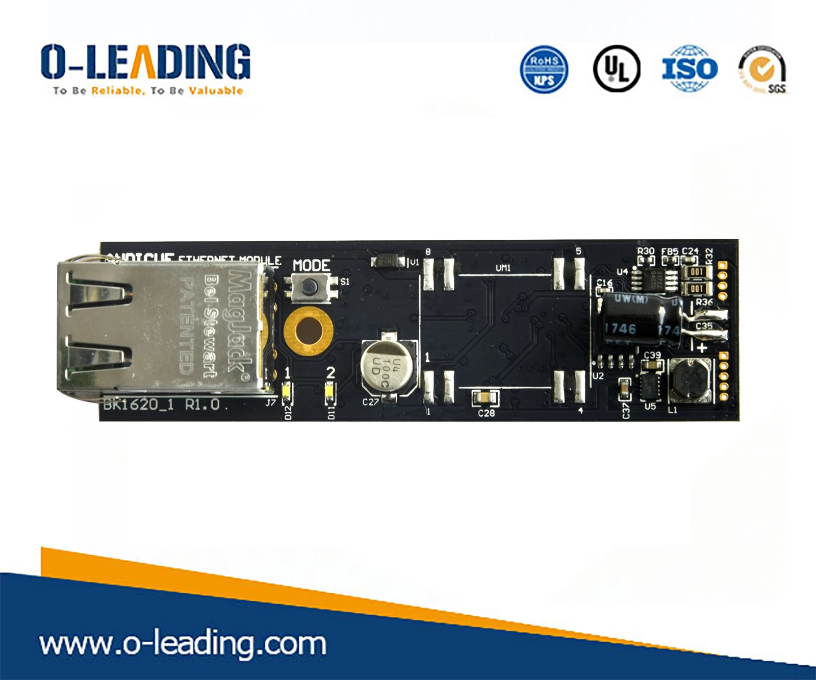
However, in mass-produced factories, there is no way for you to use the meter to slowly measure whether each resistor, capacitor, inductor, or even IC circuit on each board is correct, so there is so-called ICT automation. The appearance of the test machine, which uses multiple probes to simultaneously touch all the parts of the board that need to be measured, and then sequentially measure the characteristics of these electronic parts by program-controlled, side-by-side, usually test It takes only about 1~2 minutes for all the parts of the board to be completed. Depending on the number of parts on the board, the more parts, the longer the parts. GOLDEN FINGER BOARD supplier.
However, if these probes are directly exposed to the electronic parts on the board or their soldering feet, it is likely to crush some electronic parts, but it is counterproductive, so the clever engineers invented the test points and extra leads at the ends of the parts. A pair of small dots with no solder mask on them allow the test probe to touch these small dots without directly touching the electronic components being measured.
In the early days when the board was also in the traditional plug-in (DIP) era, the soldering feet of the parts were used as test points. Because the soldering feet of the traditional parts are strong enough, they are not afraid of pinning, but there are often probes. The misjudgment of poor contact occurs because the general electronic parts after wave soldering or SMT tinning often form a residual film of solder paste on the surface of the solder. The impedance of this film is very high, often It can cause poor contact of the probe, so the test workers who often see the production line at that time often use air spray guns to blow hard, or use alcohol to wipe the places that need to be tested.
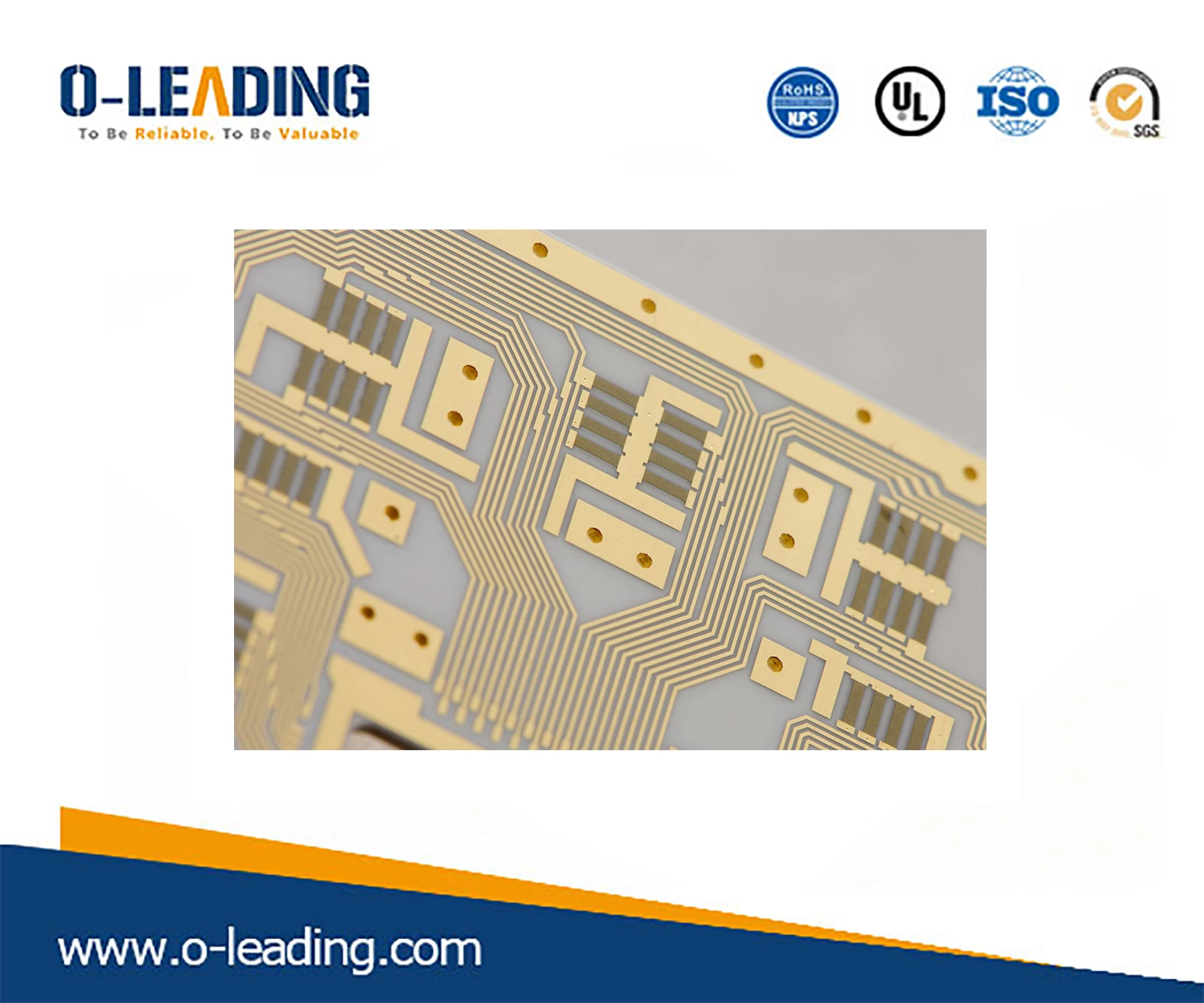
In fact, the test points after wave soldering will also have poor probe contact. Later, after SMT became popular, the test misjudgment situation was greatly improved. The application of test points was also greatly burdened, because the parts of SMT are usually very fragile and cannot withstand the direct contact pressure of the test probe. It is possible to prevent the probe from directly contacting the part and its solder fillet, not only to protect the part from damage, but also to greatly improve the reliability of the test, because the situation of misjudgment is reduced. Panel Plating Gold wholesales.
However, with the evolution of technology, the size of the circuit board is getting smaller and smaller. It is already a little difficult to squeeze so many electronic parts on the small circuit board. Therefore, the test point occupies the space of the board, often in the There is a tug-of-war between the design side and the manufacturing end, but this topic will have a chance to talk again later. The appearance of the test points is usually round, because the probes are also round, better to produce, and it is easier to get adjacent probes closer together, so that the needle density of the needle bed can be increased.