


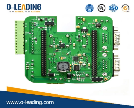
SMT wave soldering quality defects and solutions
▶ Tipping refers to the occurrence of excess needle solder at the end of the solder joint, which is a unique defect in the wave soldering process.
Causes: Improper PCB transfer speed, low preheating temperature, low tin pot temperature, small PCB transfer inclination, poor wave crest, solder failure, and poor solderability of component leads.
Solution: Adjust the transfer speed to the right, adjust the preheating temperature and tin pot temperature, adjust the PCB transfer angle, optimize the nozzle, adjust the wave shape, replace the new flux and solve the problem of lead solderability.
▶ The causes of false soldering: poor solderability of component leads, low preheating temperature, solder problems, low flux activity, too large pad holes, oxidation of the lead board, contamination on the board surface, excessive transfer speed, and solder pot temperature low.
Solution: Solve lead solderability, adjust preheating temperature, test solder tin and impurity content, adjust flux density, reduce pad holes during design, remove PCB oxide, clean board surface, adjust transfer speed, adjust tin pot temperature .
▶ Causes of thin tin: poor solderability of component leads, too large pads (except for large pads required), too large pad holes, too large soldering angles, excessive transfer speeds, high solder pot temperatures, and flux coating Unevenness and insufficient tin content in solder.
Solution: Solve the solderability of the leads, reduce the pads and pad holes, reduce the soldering angle during the design, adjust the transfer speed, adjust the temperature of the tin pot, check the pre-applied flux device, and test the solder content.
▶ Reasons for missing soldering: poor lead solderability, unstable solder wave crests, flux failure or uneven spraying, poor PCB local solderability, jitter in the transfer chain, incompatible pre-flux and flux, and unreasonable process flow.
Solution: Solve the lead solderability, check the wave device, replace the flux, check the pre-applied flux device, solve the PCB solderability (cleaning or return), check and adjust the transmission device, uniformly use the flux, and adjust the process flow.
▶ Blister film of printed board after welding
After welding, SMA will appear light green bubbles around individual solder joints. In severe cases, fingernail-sized bubbles will appear, which not only affects the appearance quality, but also affects performance in severe cases. This defect is also a reflow soldering process. Problems often occur in the medium, but more often in the wave soldering.
Cause: The root cause of the foaming of the solder mask is the existence of gas or water vapor between the solder mask and the PCB substrate. These traces of gas or water vapor will be entrained in different processes. When encountering soldering high temperature The gas expansion causes the solder mask to delaminate from the PCB substrate.When soldering, the temperature of the pad is relatively high, so bubbles first appear around the pad.
Moisture is trapped in the PCB for one of the following reasons:
PCBs often need to be cleaned and dried before the next step in the processing process.If etched, the solder mask should be applied after drying. If the drying temperature is not enough at this time, water vapor will be entrained into the next step. Bubbles appear at high temperatures.
The storage environment before PCB processing is not good, the humidity is too high, and the soldering has not been dried in time.
In the wave soldering process, water-containing flux is often used now. If the PCB preheating temperature is not enough, the moisture in the flux will enter the PCB substrate along the hole wall of the through hole. Bubbles will be generated after the high temperature of the welding.
Solution:
Strictly control all production links. The purchased PCB should be stored after inspection. Generally, the PCB should not blister within 10s at 260 ° C.
The PCB should be stored in a ventilated and dry environment, and the storage period should not exceed 6 months;
The PCB should be pre-baked in an oven at (120 ± 5) ℃ for 4 hours before soldering.
The preheating temperature in wave soldering should be strictly controlled, and it should reach 100 ~ 140 ℃ before entering the wave soldering. If a water-containing flux is used, its preheating temperature should reach 110 ~ 145 ℃ to ensure that water vapor can be evaporated.