


Causes of blistering after SMA soldering and open or false soldering of IC pins
Blister on PCB substrate after SMA soldering
After SMA welding, nail-sized bubbles appear, the main reason is that water vapor is trapped inside the PCB substrate, especially the processing of multilayer boards. Because multilayer boards are formed by pre-forming multilayer epoxy prepregs and then hot-pressing, If the storage period of the epoxy prepreg is too short, the resin content is not enough, and the pre-drying removes the water vapor and the cleaning is not clean, it is easy to entrain water vapor after hot-press molding. It may also be because of the insufficient glue content of the prepreg itself, between layers. Insufficient binding force leaves bubbles. In addition, after the PCB is purchased, the storage period is too long and the storage environment is humid. The chip is not pre-baked in time before the production of the chip, and the wet PCB is also prone to blistering.
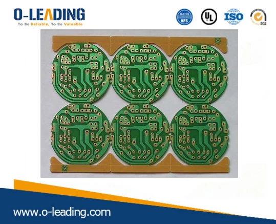
Single Side PCB manufacturer china
Solution: PCB should be checked and accepted before it can be put into storage; PCB should be pre-baked at (120 ± 5) ℃ for 4 hours before placement.
Open or dummy soldering of IC pins after soldering cause:
1.Poor coplanarity, especially FQFP devices, lead deformation due to improper storage.If the chip mounter does not have the function of checking coplanarity, it is sometimes difficult to find.
2.The solderability of the pins is not good, the IC is stored for a long time, the pins are yellow, and the solderability is poor.
3.The quality of solder paste is low, the metal content is low, and the solderability is poor. Generally, the solder content of FQFP device solder paste should be no less than 90%.
4.The preheating temperature is too high, which will easily cause the IC pins to oxidize, which will worsen the solderability.
5.The size of the printing template window is so small that the amount of solder paste is insufficient.
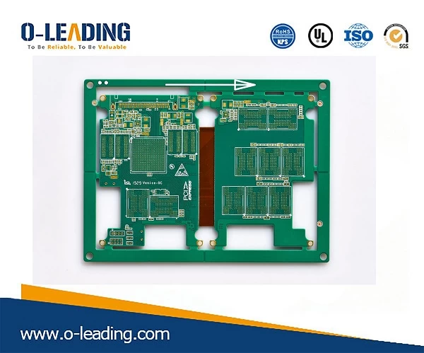
Double Side PCB manufacturer china
Solution:
1. Pay attention to the storage of the device, do not take components or open the package at will.
2.The solderability of components should be checked during production, and special attention should be paid to the storage period of the IC should not be too long (within one year from the date of manufacture), and it should not be subjected to high temperature and high humidity during storage.
3. Carefully check the template window size, it should not be too large or too small, and pay attention to match the PCB pad size