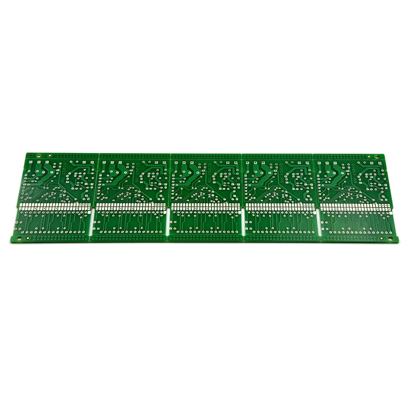
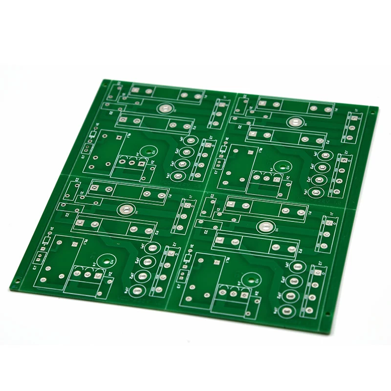
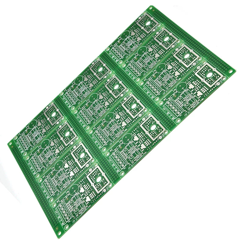
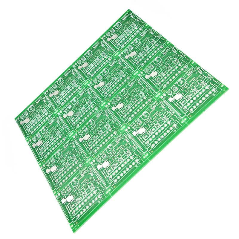
What spacing requirements do I need to pay attention to in my PCB design?
We will encounter a variety of safety clearance issues in ordinary PCB design, such as the distance between vias and pads, the distance between traces and traces, etc. are all places we should consider . So today we divide these clearance requirements into two categories, one is: electrical safety distance; the other is: non-electrical safety distance.
Electrical safety clearance
Space between wires
According to the production capacity of the PCB manufacturer, the distance between the trace and the trace must not be less than 4MIL. The minimum line spacing is also the line-to-line and line-to-pad spacing. Then, from the perspective of our production, of course, the larger the better, the better. The general 10MIL is more common.
2. Pad aperture and pad width:
According to the PCB manufacturer, if the pad hole diameter is mechanically drilled, it must be at least 0.2mm, and if it is laser-drilled, it must be at least 4mil. The hole tolerance varies slightly depending on the plate. Generally can be controlled within 0.05mm. The minimum pad width must be at least 0.2mm.
3. Pad-to-pad spacing:
According to the processing ability of the PCB manufacturer, the distance between the pad and the pad must not be less than 0.2MM.
4. The distance between the copper sheet and the board edge:
The distance between the charged copper skin and the edge of the PCB is preferably not less than 0.3mm. If the copper is laid over a large area, there is usually a shrinkage distance from the edge of the board, which is generally set to 20mil. In general, due to mechanical considerations of the finished circuit board, or to avoid possible curling or electrical shorts caused by the bare copper on the edge of the board, engineers often shrink large-area copper blocks by 20mil relative to the edge of the board. Instead of laying the copper all the way to the edge of the board. There are many ways to deal with copper shrinkage. For example, draw the keepout layer on the edge of the board, and then set the distance between the copper and keepout.
Non-electrical safety clearance
1. Character width and height and spacing:
As for the characters of silk screen, we generally use conventional values such as: 5/30 6/36 MIL. Because when the text is too small, the printing will be blurred.
2. Distance from silk screen to pad:
Silk screen is not allowed on the pad. Because if the silk screen is covered with a pad, the silk screen cannot be tinned when the solder is applied, which affects the component mounting. Generally, the board factory requires 8mil space. If it is because some PCB board area is very close, we can achieve 4MIL spacing is barely acceptable. Then, if the silk screen accidentally covers the pad during design, the board factory will automatically eliminate the silk screen part left on the pad during manufacturing to ensure the tin on the pad. So we need to pay attention.

3. 3D height and horizontal distance on the mechanical structure:
When mounting devices on the PCB, consider whether there will be conflicts with other mechanical structures in the horizontal direction and space height. Therefore, in the design, we must fully consider the adaptability of the space structure between the components and between the finished PCB and the product shell, and reserve a safe distance for each target object.


