


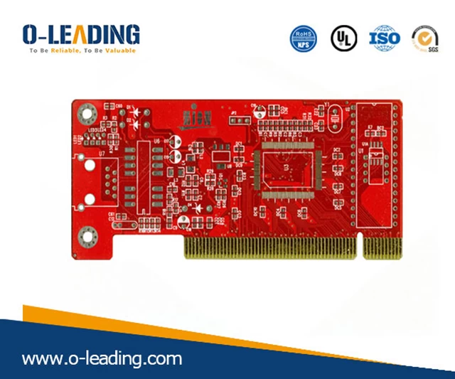
Printed circuit board manufacturing process
Laser drilling manufacturer china
Laminated
A new material called a prepreg is needed here, which is the core and core board (>2 layers of PCB), and the adhesive between the core board and the outer layer of copper foil, and also acts as an insulator.
The lower layer of copper foil and the two layers of prepreg have been fixed in advance through the alignment hole and the lower iron plate, and then the prepared core plate is also placed in the alignment hole, and finally two layers of prepreg, a layer of copper foil and A layer of pressure-bearing aluminum plate covers the core.
The PCB boards sandwiched by the iron plates are placed on the holders and then fed into a vacuum hot press for lamination. The high temperature in the vacuum hot press melts the epoxy in the prepreg and holds the core and copper foil under pressure.
After the lamination is completed, the upper iron plate of the pressed PCB is removed. The pressure-bearing aluminum plate is then removed, and the aluminum plate also serves to isolate the different PCBs and ensure the smoothness of the outer copper foil of the PCB. Both sides of the PCB taken out at this time will be covered by a layer of smooth copper foil.
Drilling
To connect the four layers of copper foil that are not in contact with each other in the PCB, first drill the perforations through the top and bottom to open the PCB, and then metallize the holes to conduct electricity.
The X-ray drilling machine is used to position the inner core board. The machine will automatically find and locate the hole on the core board, and then position the PCB with a positioning hole to ensure that the next hole is drilled from the center of the hole. Over.
Place a layer of aluminum on the puncher machine and place the PCB on top. In order to improve efficiency, 1 to 3 identical PCB boards are stacked together for perforation according to the number of layers of the PCB. Finally, the topmost PCB is covered with an aluminum plate. The upper and lower layers of the aluminum plate are used to not tear the copper foil on the PCB when the drill bit is drilled and drilled.
In the previous lamination process, the melted epoxy was extruded outside the PCB, so removal was required. The die milling machine cuts the periphery of the PCB according to the correct XY coordinates of the PCB.
Copper chemical precipitation of pore walls
Since almost all PCB designs are lines of different layers that are connected by perforations, a good connection requires a 25 micron copper film on the hole walls. This thickness of copper film needs to be achieved by electroplating, but the walls of the holes are composed of non-conductive epoxy and fiberglass sheets.
So the first step is to first deposit a layer of conductive material on the wall of the hole, and form a 1 micron copper film on the entire surface of the PCB, including the hole wall, by chemical deposition. The entire process, such as chemical processing and cleaning, is controlled by the machine.
Outer PCB layout transfer
Next, the outer PCB layout will be transferred to the copper foil. The process is similar to the previous inner core PCB layout transfer principle. The photocopying film and photosensitive film are used to transfer the PCB layout to the copper foil, the only difference. It will be a positive film.
The transfer of the inner layer PCB layout is a subtractive method, which uses a negative film. The circuit covered by the cured photosensitive film on the PCB is used to clean away the unsolidified photosensitive film, and after the exposed copper foil is etched, the PCB layout line is protected by the cured photosensitive film.
The transfer of the outer PCB layout is based on the normal method, using a positive film. The cured film on the PCB is covered by a non-line area. Electroplating is performed after cleaning the uncured photosensitive film. There is no film at the film, and there is no film, first plated with copper and then tin plated. After the film is removed, alkaline etching is performed, and finally tin is removed. The line pattern remains on the board because it is protected by tin.
Clamp the PCB with a clip and plate the copper. As mentioned before, in order to ensure that the hole position has sufficient conductivity, the copper film plated on the hole wall must have a thickness of 25 microns, so the whole system will be automatically controlled by the computer to ensure its accuracy.
Outer PCB etching
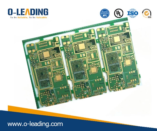
The etching process is then completed by a complete automated pipeline. First, the cured film on the PCB is washed away. The undesired copper foil covered by it is then washed away with a strong alkali. The tin plating on the PCB layout copper foil is removed by using tin-removing liquid. After cleaning, the 4-layer PCB layout is complete.