


PCB industry productive technology development trend
The copper layer on the surface of the PCB needs to be protected in order to prevent oxidation and deterioration of the copper, providing a reliable connection surface during assembly.
Some commonly used surface finishes in PCB manufacturing include lead- or lead-free hot air leveling solder, immersion tin, organic solderability protective film, electroless nickel/gold plating, electroplated nickel/gold, and the like.
The surface finish of HDI boards and IC package carriers has evolved from electroless nickel/gold (ENIG) to electroless nickel/palladium/gold (ENEPIG), which helps prevent black discs from appearing after component mounting and affects reliability.
The palladium layer in the ENEPIG coating has been analyzed. The palladium layer structure has pure palladium and palladium phosphorus alloys, which have different hardnesses. Therefore, it is necessary to select different palladium layers for wire bonding and for welding.
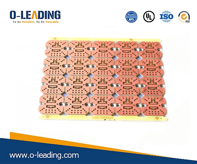
Immersion Gold manufacturer China
After the reliability impact assessment, the presence of trace amounts of palladium increases the thickness of copper-tin growth; while the excessive palladium content produces a brittle palladium-tin alloy, which in turn reduces the strength of the solder joints, thus requiring proper palladium thickness.
From the perspective of the fine line of the PCB, the surface treatment uses electroless palladium/immersion gold (EPIG) to be better than electroless nickel/palladium/immersion gold (ENEPIG), reducing the effect on fine line width/line spacing. EPIG coatings are thinner and do not cause line distortion; EPIG can meet soldering and wire bonding tests.
There are also new direct electroless palladium plating (EP) or direct immersion gold (DIG) on copper, or electroless palladium and autocatalytic gold plating (EPAG) coating on copper, which has the advantage of being suitable for the pressure bonding of gold wire or copper wire. Because there is no nickel layer and there is better high frequency characteristics, the coating is thin and more suitable for fine line patterns, and the process and cost are reduced.
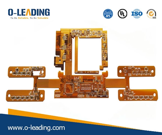
Buried vias manufacturer China
Improvements in the final finish of the PCB, in addition to the introduction of electroless nickel-plated silver (NiAg) coating, silver has good electrical conductivity, solderability, nickel corrosion resistance. The organic coated OSP is improved in properties to improve heat resistance and weldability. There is also an organic-metal composite (OM) coating that has a good price/performance ratio for coating the OM coating on the copper surface of the PCB.
Clean manufacturing
“Green” and “environmentally friendly” are now important signs of PCB manufacturing technology advancement. In addition to trying to adopt revolutionary clean production technologies such as printed electronics and 3D printing, the improvement of existing PCB manufacturing technology to cleaner production is ongoing. Such as the search for materials to replace toxic and hazardous substances, reduce processing steps, and reduce the consumption of chemicals, as well as reduce the amount of water and energy, and the recycling of materials.
Specifically, non-toxic inorganic materials are used as flame retardants, and halogen-free substrates such as electrical, thermal conductivity, and thermal expansion coefficient are also improved; direct laser imaging is used to reduce work processes and material consumption; and semi-additive method is used to reduce electroplating copper and The consumption of etched copper; the use of direct metallization hole process, and the elimination of toxic and harmful substances in the chemical copper bath; the conductive paste printing makes the via hole interconnection process clean and simple.
Direct metallization technology has existed for a long time, and its development has matured over the years. The direct metallization process has a carbon black system and a conductive polymer system, which is activated by carbon or graphite or a conductive polymer instead of palladium, and the toxic formaldehyde, cyanide and refractory EDTA complexing agent are eliminated in the chemical copper bath.
The introduction of colloidal graphite direct pore metallization technology has stable dispersibility and good adsorption with a variety of resins. The colloidal graphite direct metallization process has been used in rigid PCB manufacturing for many years. It can now be applied to HDI boards, flexible boards and rigid-flex boards with complex blind holes, buried holes and any layer interconnections, which can reduce process and equipment sites and wastewater. The quantity is beneficial to the environment and enhances the production efficiency and the high reliability of the final product.
Once known as waste or even hazardous waste in PCB production, it is no longer a “waste”. For example, the excess copper etching solution, the micro etching treatment liquid, and the plating cleaning liquid tend to be recycled online. Some newly designed production line equipment.
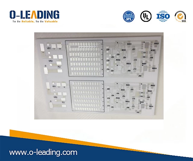
PCB Assembly manufacturer China
Whether it is etched lines or vertical plating lines and horizontal plating lines, have been considered to be equipped with on-line recycling and regenerative devices, as well as reasonable configuration of air-to-zone between sections, energy saving of circulating pumps, automatic analysis and addition of liquids.
Measures such as the life of the liquid medicine are not only conducive to improving quality, but also conducive to energy conservation and environmental protection.