


PCB process manufacturing future trends
The history of printed electronics is very early, but it has only prospered in recent years. Printed electronics is used in the printed circuit industry as part of printed circuit technology.
Multiple Flex-Rigid Board factory
The continuous development of printed electronics shows that the prospects for commercial applications are very broad. Now PCB manufacturers have invested in printed electronics. They started with flexible boards and replaced printed circuit boards (PCBs) with printed electronic circuits (PEC). Printed electronic technology is closest to FPCB. At present, there are many substrates and ink materials. Once the performance and cost are broken, it will be applied in a large amount, and the cost reduction will open up a larger market.
A hybrid system of organic and printed electronics helps the industry grow. The hybrid system of traditional silicon and printed electronic components, which may open up a new PCB industry. These hybrid technologies include large area lithography, screen printing or inkjet printing, and flexible PCB technology.
An important aspect of printed electronics is materials, including substrates and functional inks. In addition to the existing FPCB, flexible substrates also develop higher performance substrates. Currently, there are high dielectric substrate materials composed of a mixture of ceramic and polymer resins, as well as high temperature substrates, low temperature substrates and colorless transparent substrates. , yellow substrate, etc.
In addition to some polymer materials, printed electronics also require functional ink materials, mainly conductive inks, which are constantly improving the conductivity, printing adaptability and low cost. Currently, conductive inks are available for printing electronic products. There are many types. In addition, there are piezoelectric, thermoelectric, and ferroelectric materials that can be used in combination in printed electronics to achieve versatility.
Laser drilling manufacturer china
Another important aspect of printed electronics is the printing process and the corresponding printing equipment, which is an innovative development of traditional printing technology. Printed electronics can be applied to different printing methods such as gravure, letterpress, screen printing and inkjet printing. Screen printing has been applied in PCB manufacturing, with mature technology and low cost. Currently, it is developing towards automation and high definition.
The range of applications of inkjet printing in PCB manufacturing is expanding, from marking symbols, solder resists to resist patterns, to further direct the printing of conductive patterns; at the same time, inkjet printing is highly refined and rapidly developed. For example, the new aerosol spray technology is significantly superior to piezoelectric spray printing, forming wires with fine and three-dimensional requirements, and can directly print electronic circuits and components on planar or three-dimensional members.
There is also a method of inkjet printing using laser irradiation to instantaneously cure the ink. The thickness and width of the conductive line are more than 1.0, such as a line width of 10 μm and a line height of 10 μm. For example, a line width of 30 μm and a line thickness of 20 μm are formed on the PI film. FPCB.
The current focus of printed electronics is the low-cost manufacturing of radio frequency identification (RFID) tags that can be printed in rolls. Potential is the field of printed displays, lighting and organic photovoltaics. The wearable technology market is currently a favorable market.
Wearable technology products such as smart clothing and smart sports glasses, activity monitors, sleep sensors, smart watches, enhanced realistic headphones, navigation compass and more. Wearable technology devices are indispensable for flexible electronic circuits, which will drive the development of flexible printed electronic circuits.
Embedded component printed circuit technology
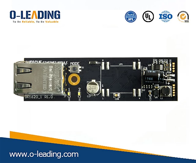
Net Power Module manufacturer china
Embedded Component Printed Circuit Board (EDPCB) is a product that enables high-density electronic interconnects. Buried component technology has great potential in PCBs. Buried component PCB manufacturing technology enhances the functionality and value of PCBs, in addition to applications in communications products, but also provides opportunities in automotive, medical, and industrial applications.
The development of EDPCB, from printed resistors made of carbon paste and thin film resistors made of nickel-phosphorus alloy foil, and planar capacitors with high dielectric constant substrates, to form embedded passive component printed boards, into embedded ICs The chip and the embedded chip component form a buried active and passive component printed board. The problems faced today are the complexity of embedded components and the thinning of EDPCB, as well as heat dissipation and thermal deformation control, and final inspection technology.
Component embedding technology is now used in portable terminal devices such as mobile phones. The EDPCB manufacturing process enters the practical B2it method, which can achieve high reliability and low cost; there is a PAPAL method, which achieves high-level and low power consumption, and is used in automotive electronics; there is a communication module in which a wafer-level package chip is embedded. Reflecting good high-frequency characteristics, there will be eWLB embedded with BGA chips in the future. With the establishment of EDPCB design rules, such products will develop rapidly.