


PCB technology trends are developing
Thin line
PCBs are all developed to high-density thin-line, and HDI boards are particularly prominent. The definition of HDI board a decade ago was that the line width/line spacing was 0.1 mm/0.1 mm and below, and now the industry is basically 60 μm and the advanced is 40 μm.
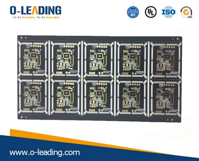
Multilayer PCB manufacturer in china
PCB circuit pattern formation, the traditional is the photo-imaging chemical etching process (subtraction method) on the copper foil substrate. This practice has many processes, is difficult to control, and has high costs. Current fine line fabrication tends to be semi-additive or improved semi-processed.
The bonding force between the conductor and the insulating substrate is customary by increasing the surface roughness to increase the surface area and improving the bonding force, such as strengthening the surface of the roughened resin layer by decontamination treatment, and treating the copper surface with high profile copper foil or oxidation. For thin wires, this physical method guarantees that bonding is not acceptable. Thus, a copper-plated high-bonding copper foil on a smooth resin surface was developed. If there is a "molecular bonding technique", the surface of the resin substrate is chemically treated to form a functional group which can be closely bonded to the copper layer.
In addition, the dry film imaging pattern transfer during the thin line production process, the surface treatment of copper foil is one of the key factors for success. The best combination of surface cleaner and microetcher is used to provide a clean surface with sufficient area to promote dry film adhesion. The surface anti-tarnish treatment layer of the copper foil is removed by chemical cleaning, and the dirt and oxide are removed, and an appropriate chemical cleaner is selected according to the type of the copper foil, followed by micro-etching the surface of the copper foil. In order to make the imaged dry film and the copper layer, the solder resist pattern and the thin line reliable, a method of non-physically roughening the surface should also be adopted.
Semi-additive laminate substrate
At present, the semi-additive method hotspot is to use an insulating dielectric film to laminate, and SAP is more advantageous than MSAP from the fine line implementation and manufacturing cost. The SAP laminate uses a thermosetting resin to form via holes and circuit patterns by laser drilling of copper.
At present, international HDI laminate materials use epoxy resin with different curing agents, adding inorganic powder to improve material rigidity and reduce CTE, and also use fiberglass cloth to enhance rigidity.
Copper plated hole
For reliability reasons, interconnect holes are made of electroplated copper fillet technology, including blind via copper and via fill copper.
The ability to fill copper holes is in the filling: whether there are voids in the holes closed by copper; flatness: the degree of dimple in the copper-plated opening; thickness-to-diameter ratio: thickness (hole depth) and aperture proportion.
Inverted chip package IC package carrier board technology
Organic substrates in global semiconductor packaging account for more than one-third of the market. As the production of mobile phones and tablets increased, FC-CSP and FC-PBGA increased significantly. The package carrier replaces the ceramic substrate with an organic substrate, and the pitch of the package carrier is getting smaller and smaller, and the typical line width/line pitch is now 15 μm.
Future development trends. The BGA and CSP fine pitch carrier will continue, while the coreless board and four or more layers of carrier board will be more used. The roadmap shows that the carrier board has smaller feature sizes, and the performance focus requires low dielectric and low. The coefficient of thermal expansion and high heat resistance pursue a low-cost substrate based on meeting performance targets.
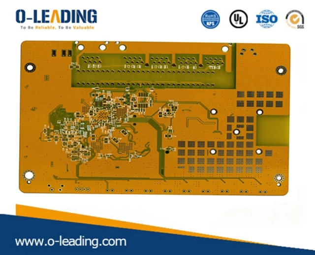
Printed circuit boards supplier
Adapt to high-frequency and high-speed requirements
Electronic communication technology ranges from wired to wireless, from low frequency, low speed to high frequency and high speed. Now the performance of mobile phones has entered 4G and will move towards 5G, which means faster transmission speed and larger transmission capacity. The arrival of the global cloud computing era has doubled the data traffic, and the high-speed and high-speed communication equipment is an inevitable trend. PCB is suitable for high-frequency, high-speed transmission. In addition to reducing signal interference and loss in circuit design, maintaining signal integrity, and PCB manufacturing to meet design requirements, it is important to have high-performance substrates.
In order to solve the increase in speed and signal integrity of the PCB, it is mainly for the electrical signal loss attribute. The key factors for substrate selection are dielectric constant (Dk) and dielectric loss (Df). When Dk is lower than 4 and Df is less than 0.010, it is a medium Dk/Df laminate. When Dk is lower than 3.7 and Df is less than 0.005, it is low Dk/. Df grade laminate.
The surface roughness (profile) of the conductor copper in high-speed PCBs is also an important factor affecting signal transmission loss, especially for signals above 10 GHz. Copper foil roughness needs to be less than 1 μm at 10 GHz, and the use of ultra-planar copper foil (surface roughness 0.04 μm) is more effective.