


Technical PCB multi-layer board details
With the continuous development of SMT (Surface Mount Technology) and the continuous introduction of new generation SMD (surface mount devices), such as QFP, QFN, CSP, BGA (especially MBGA), electronic products are more intelligent and miniaturized. Promoted major reforms and advancements in PCB industry technology. Since IBM first successfully developed high-density multilayer boards (SLCs) in 1991, various national groups have also developed a variety of high-density interconnect (HDI) microplates. The rapid development of these processing technologies has prompted the development of PCBs to gradually move toward multi-layer, high-density wiring. Multi-layer printed boards are widely used in the manufacture of electronic products due to their flexible design, stable and reliable electrical performance and superior economic performance.
1 Signal layers
AlTIum Designer provides up to 32 signal layers, including Top Layer, Bottom Layer, and Mid-Layer. The layers can be interconnected by vias, blind vias, and buried vias.
(1) Top Layer
Also called component layer, mainly used to place components, for double-layer boards and multi-layer boards can be used to arrange wires or copper.
(2)Bottom Layer
Also known as solder layer, mainly used for wiring and soldering, for double-layer boards and multi-layer boards can be used to place components.
(3) Mid-Layers
There are up to 30 layers, which are used to lay out signal lines in the multi-layer board. Power lines and ground lines are not included here.
2 Internal Planes
Usually referred to as the inner layer, it only appears in the multi-layer board. The number of layers of the PCB board generally refers to the sum of the signal layer as well as the inner layer. Similar to the signal layer, the inner and inner layers, the inner layer and the signal layer can be connected to each other through holes, blind holes and buried holes.
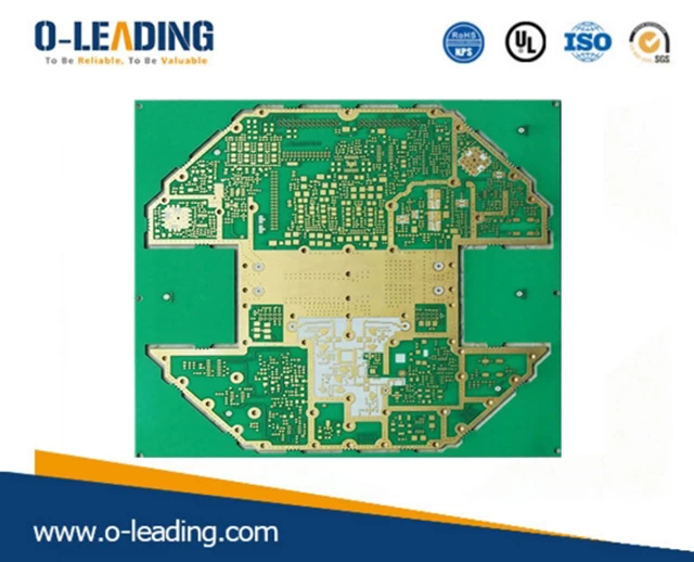
Multilayer pcb manufacturer china
3 Silkscreen Layers
A PCB board can have up to 2 silk screen layers, which are Top Overlay and Bottom Overlay, which are generally white. They are mainly used for placing printed information, such as the outline and label of components. A note character, etc., to facilitate the soldering and circuit inspection of PCB components.
(1) Top Overlay
Used to mark the projected outline of the component, the label of the component, the nominal value or model number, and various comment characters.
(2) Bottom Overlay
Same as the top silkscreen layer, if all the labels are included in the top silkscreen layer, the underlying silkscreen layer can be closed.
4 Mechanical Layers
Mechanical layers are generally used to place instructive information about the board and assembly methods, such as PCB dimensions, dimensional markings, data sheets, via information, and assembly instructions. This information varies depending on the requirements of the design company or PCB manufacturer. The following examples illustrate our common methods.
Mechanical 1: Generally used to draw the border of the PCB, as its mechanical shape, it is also called the shape layer;
Mechanical 2: We use the table to process the PCB processing requirements, including dimensions, plates, and layers.
Mechanical 13 & Mechanical 15: The body size information of most components in the ETM library, including the 3D model of the component; this layer is not displayed by default for the simplicity of the page;
Mechanical 16: The footprint information of most components in the ETM library can be used to estimate the PCB size early in the project; for the simplicity of the page, the layer is not displayed by default and the color is black.
china Rigid-flexible pcb on sale
5, Mask Layers
AlTIum Designer offers two types of Mask Layers, the Solder Mask and the Paste Mask, in which there are two layers, the top layer and the bottom layer, which are not described in detail here.