


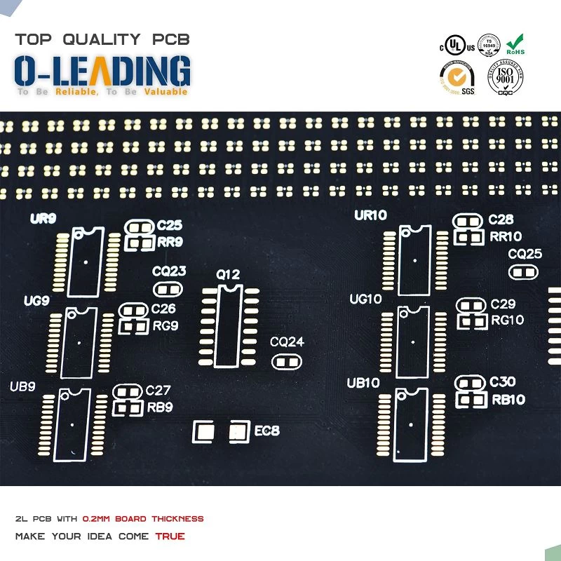
How is the high precision of PCB made?
The high-precision circuit board refers to the use of fine line width/spacing, small holes, narrow ring width (or no ring width), and buried and blind holes to achieve high density. High precision means that the result of "fine, small, narrow, and thin" will inevitably lead to high precision requirements. Take the line width as an example: 0.2mm line width, 0.16~0.24mm is qualified as required, and the error is (0.20 ± 0.04) mm; while the line width of 0.10 mm, the error is (0.10 ± 0.02) mm, obviously the accuracy of the latter is doubled.
Fine wire technology
In the future, the high-density line width/spacing will be 0.2mm-0.13mm-0.08mm-0.05mm to meet the requirements of SMT and multi-chip packaging (MCP).
Therefore, the following technologies are required:
①Using thin or ultra-thin copper foil (<18um) substrate and fine surface treatment technology.
②Using thinner dry film and wet filming process, thin and good quality dry film can reduce line width distortion and defects. Wet film can fill small air gaps, increase interface adhesion, and improve wire integrity and accuracy.
③Using electrodeposited photoresist film (ED). Its thickness can be controlled in the range of 5-30/um, and it can produce more perfect fine wires. It is especially suitable for narrow ring width, no ring width and full plate electroplating. At present, there are more than ten ED production lines in the world.
High Precision Manufacturing OEM Flex Rigid Flexible Pcb
④Using parallel light exposure technology. Since the parallel light exposure can overcome the influence of the line width variation caused by the oblique rays of the "point" light source, it is possible to obtain fine wires with precise line width dimensions and smooth edges. However, the parallel exposure equipment is expensive, the investment is high, and it is required to work in a highly clean environment.
⑤Using automatic optical inspection technology (AOI). This technology has become an indispensable means of detection in the production of fine wires, and is rapidly being promoted, applied and developed.
OEM electronic printed circuit board manufacturer electronic controller board
The functional holes of the printed boards used for surface mounting of the microporous technology are mainly used for electrical interconnection, which makes the application of microporous technology more important. Using conventional drill materials and CNC drilling machines to produce tiny holes has many failures and high costs. Therefore, the high-density of printed boards is mostly focused on the refinement of wires and pads. Although great results have been achieved, its potential is limited. To further improve the density (such as wires less than 0.08mm), the cost is soaring. , So turn to use micropores to improve densification.