


Three common drilling holes (through holes, blind holes, buried holes) in PCB circuit boards
The purpose of PCB drilling is to drill through holes that connect the lines between layers on the board.
Via: This is a common hole used to conduct or connect copper foil lines between conductive patterns in different layers of the circuit board. For example (such as holes, buried holes), but can not insert component leads or copper-plated holes of other reinforcing materials.
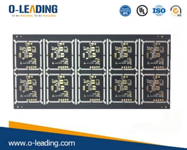
Printed circuit board manufacturer China
The characteristic is: in order to meet the needs of customers, the through hole of the circuit board must be plugged. In this way, in changing the traditional aluminum plugging process, the white mesh completes the solder mask and plugging of the circuit board surface to make the production stable and quality Reliable and perfect to use. Vias mainly play the role of interconnection and conduction of circuits. With the rapid development of the electronics industry, higher requirements have been placed on the process and surface mount technology of printed circuit boards. The process of plugging via holes is applied and should meet the following requirements:
1. There is copper in the via hole, and the solder mask can be plugged or not.
2. There must be tin and lead in the through hole, and there is a certain thickness requirement (4um) that no solder mask ink can enter the hole, resulting in hidden tin beads in the hole.
3. The through holes must have solder mask ink plug holes, opaque, and must not have tin rings, tin beads, and flatness requirements.
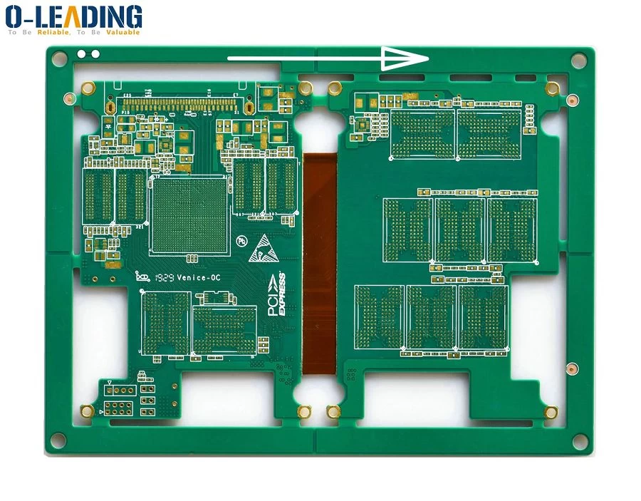
Factory Price multilayer rigid flexible HDI PCB Circuit Board
Blind hole: It is to connect the outermost circuit in the PCB with the adjacent inner layer by plating holes. Because the opposite side cannot be seen, it is called blind pass. At the same time, in order to increase the space utilization between PCB circuit layers, blind holes are applied. That is, a via hole to one surface of the printed board.
Features: Blind holes are located on the top and bottom surfaces of the circuit board, with a certain depth, used for the link between the surface circuit and the inner circuit below, the depth of the hole usually does not exceed a certain ratio (aperture). This production method requires special attention to the depth of the drilling (Z axis) to be just right. If you do not pay attention, it will cause difficulties in plating in the hole, so almost no factory adopts it. It is also possible to place the circuit layers that need to be connected in advance in the individual circuit layers. The holes are drilled first, and then glued together, but more precise positioning and alignment devices are required.
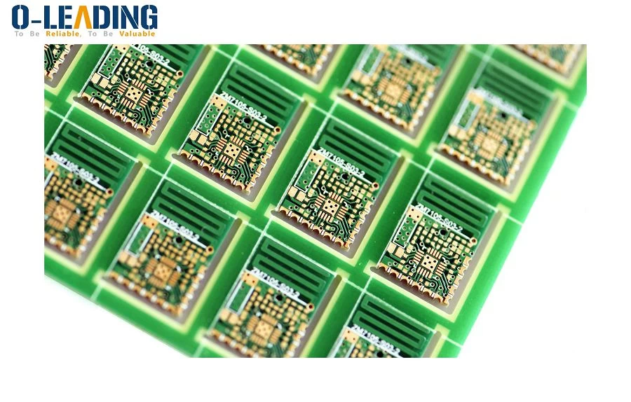
Half hole PCB module manufacturer
Buried via: It is the link between any circuit layers inside the PCB but not connected to the outer layer, and it also means a via hole that does not extend to the surface of the circuit board.
Features: This process cannot be achieved by drilling after bonding. It is necessary to perform drilling on individual circuit layers. First, the inner layer is partially bonded and then electroplated first. Finally, all bonding can be achieved, which is more conductive than the original Holes and blind holes take more time, so the price is the most expensive. This process is usually only used for high-density circuit boards to increase the usable space of other circuit layers. In the PCB production process, drilling is very important and should not be careless. Because drilling is to drill the required through holes on the copper clad board to provide electrical connections and fix the function of the device. If the operation is improper, there will be problems in the via process, and the device cannot be fixed on the circuit board, which will affect the use, and the whole board will be scrapped. Therefore, the drilling process is very important.