Why do the optoelectronic components on the PCB always fail?
As the carrier of various components and the hub of circuit signal transmission, PCB has become the most important and critical part of electronic information products. The quality and reliability of PCB determine the quality and reliability of the whole equipment.
With the miniaturization of electronic information products and the environmental protection requirements of lead-free and halogen-free, PCBs have also developed in the direction of high density and high Tg and environmental protection. However, due to cost and technical reasons, a large number of failures have occurred in the production and application process of PCBs, which has caused many quality disputes. In order to understand the cause of failure in order to find a solution to the problem and clarify responsibilities, failure analysis must be performed on the failure cases that occurred.
Basic Procedure for Failure Analysis
To obtain the exact cause or mechanism of PCB failure or failure, basic principles and analysis procedures must be adhered to, otherwise valuable failure information may be missed, causing analysis to fail to continue or may lead to erroneous conclusions. The general basic process is to first determine the failure location and failure mode through information collection, functional testing, electrical performance testing, and simple visual inspection based on the failure phenomenon, that is, failure location or fault location.
For a simple PCB or PCBA, the location of the failure is easy to determine. However, for more complex BGA or MCM packaged devices or substrates, defects are not easy to observe through a microscope, and it is not easy to determine them at this time. At this time, other means are needed to determine.
The next step is to analyze the failure mechanism, that is, use various physical and chemical methods to analyze the mechanism that causes PCB failure or defect generation, such as soldering, pollution, mechanical damage, wet stress, dielectric corrosion, fatigue damage, CAF or ion migration, Stress overload and so on.
Then there is the failure cause analysis, which is based on the failure mechanism and process analysis to find the cause of the failure mechanism. If necessary, test verification is performed. Generally, test verification should be performed whenever possible. Through test verification, the accurate induced failure cause can be found.
This provides a targeted basis for the next improvement. Finally, based on the test data, facts and conclusions obtained in the analysis process, a failure analysis report is prepared, which requires the reported facts to be clear, logical reasoning, and methodical. Don't imagine in imagination.
In the process of analysis, pay attention to the basic principles of using analytical methods from simple to complex, from outside to inside, from not destroying the sample to using the damage. Only in this way can you avoid losing critical information and avoid introducing new artificial failure mechanisms.
It is like a traffic accident. If one side of the accident destroys or flees the scene, it is difficult for the police in smart to make an accurate determination of the responsibility. At this time, traffic regulations generally require the fugitive or the side of the scene to assume full responsibility.
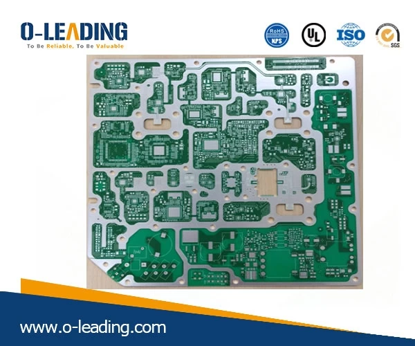
The failure analysis of PCB or PCBA is also the same. If you use a soldering iron to repair the failed solder joints or use a large scissors to cut the PCB strongly, then the analysis can no longer be started, and the failure site has been destroyed. Especially in the case of a small number of failure samples, once the environment of the failure site is destroyed or damaged, the real cause of failure cannot be obtained.


