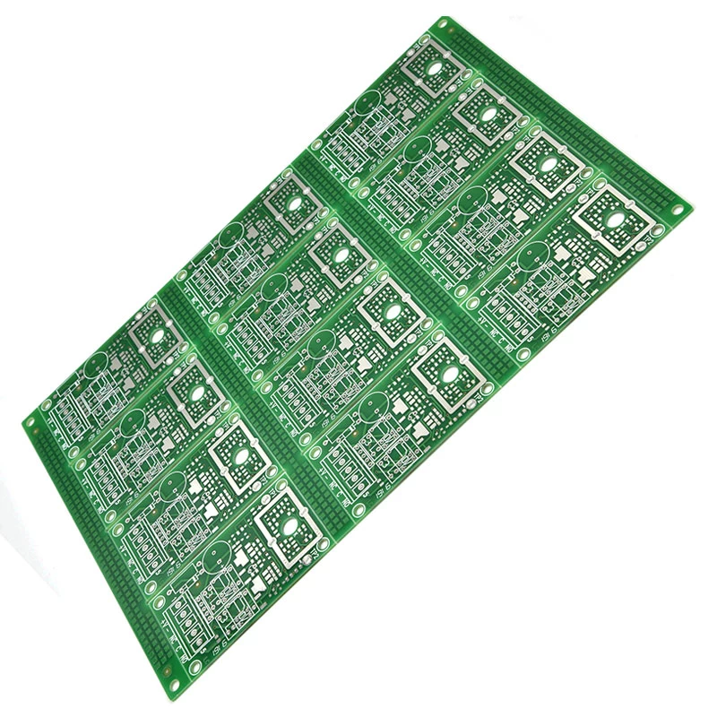
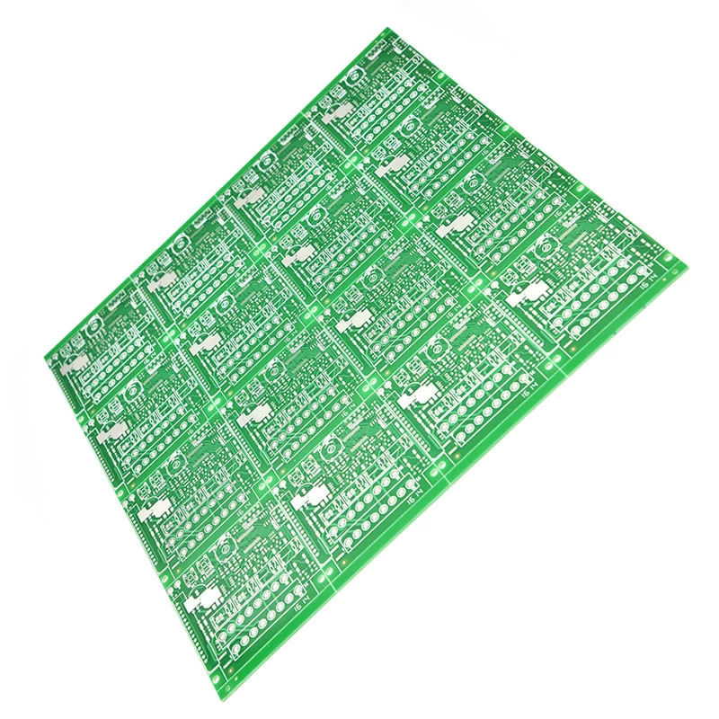
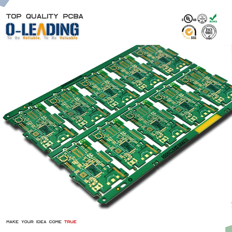
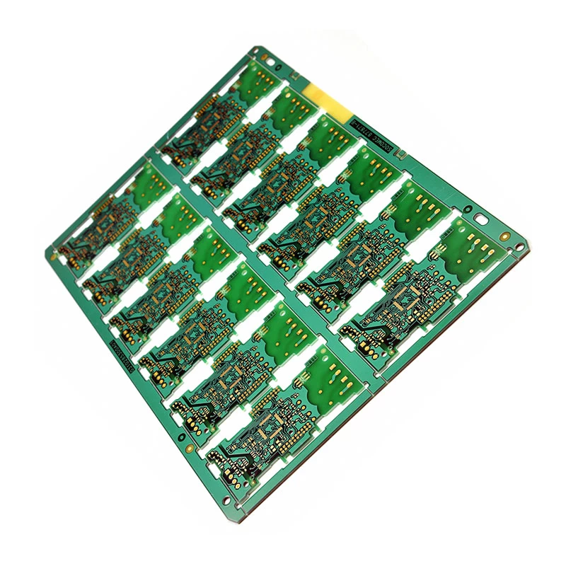
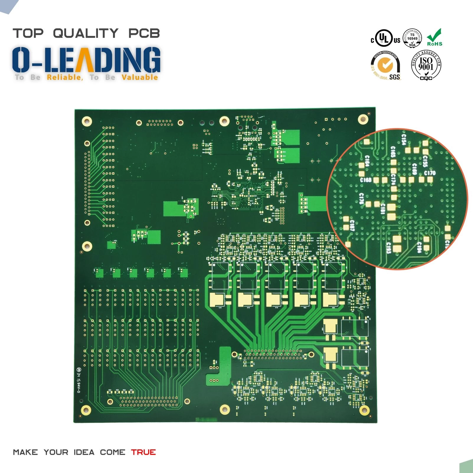
Why is the PCB circuit board via blocked?
Via holes are also known as vias. In order to meet customer requirements, the vias of circuit boards must be plugged. After a lot of practice, the traditional aluminum sheet plugging process has been changed. hole. Stable production and reliable quality.
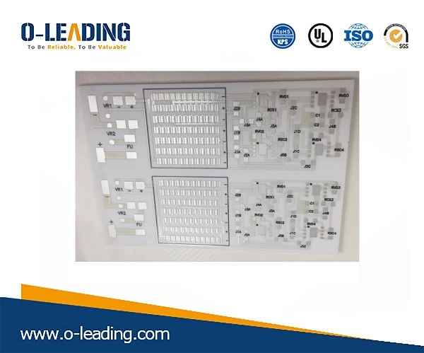
Via hole plays the role of interconnecting and connecting lines. The development of the electronics industry also promotes the development of PCBs. It also places higher requirements on printed board manufacturing processes and surface mount technology. The Via hole plugging process came into being and should meet the following requirements:
1. Copper can be used in the vias, solder plugging can be plugged or not;
2. The lead-through hole must have tin-lead, with a certain thickness requirement (4 microns), and no solder resist ink can enter the hole, causing tin beads to be hidden in the hole;
3. The through hole must be provided with a solder resist ink plug hole, which is opaque and must not have tin rings, beads, and flatness requirements.
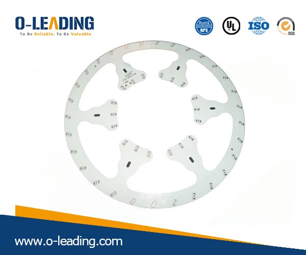
With the development of electronic products in the direction of "light, thin, short, small", PCBs have also developed to high density and high difficulty. Therefore, a large number of SMT and BGA PCBs have appeared, and customers require plugging holes when mounting components. Five roles:
1. To prevent short-circuiting of the tin from the through hole through the component surface during PCB over-wave soldering; especially when we place the via on the BGA pad, we must first plug the hole and then gold-plated to facilitate BGA welding.
2.Avoid flux residue in the via;
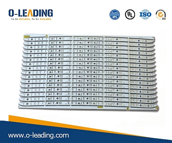
3. After the surface mounting and component assembly of the electronics factory are completed, the PCB must be vacuumed to form a negative pressure on the test machine;
4. Prevent the surface solder paste from flowing into the hole to cause false soldering and affect the placement;
5. Prevent the solder ball from popping out during over-wave soldering, causing short circuit.


