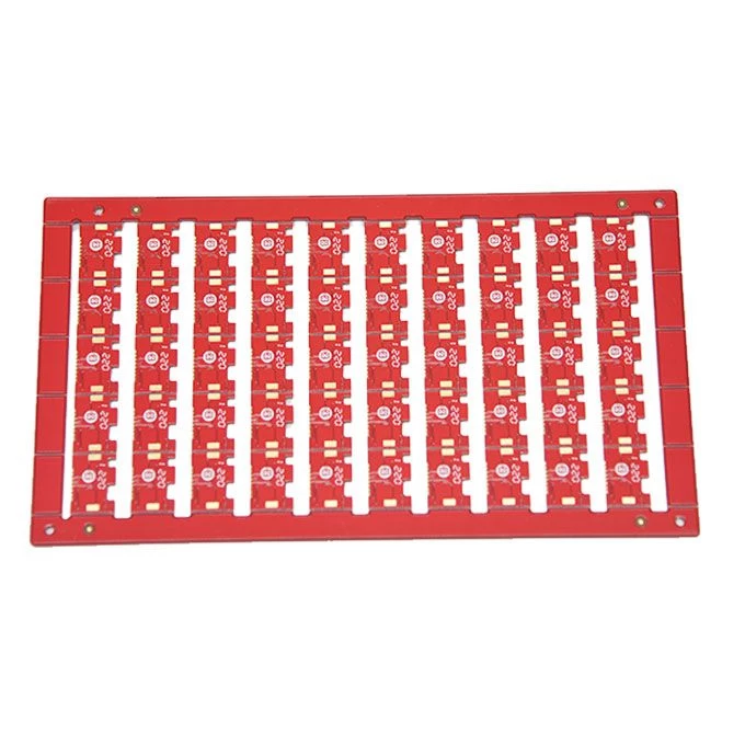
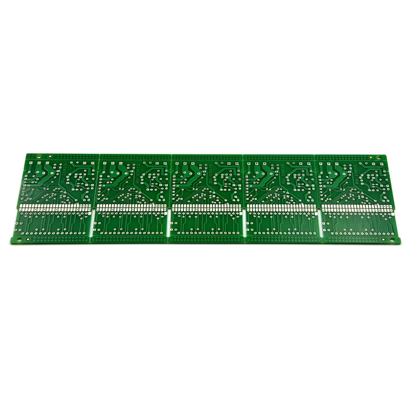
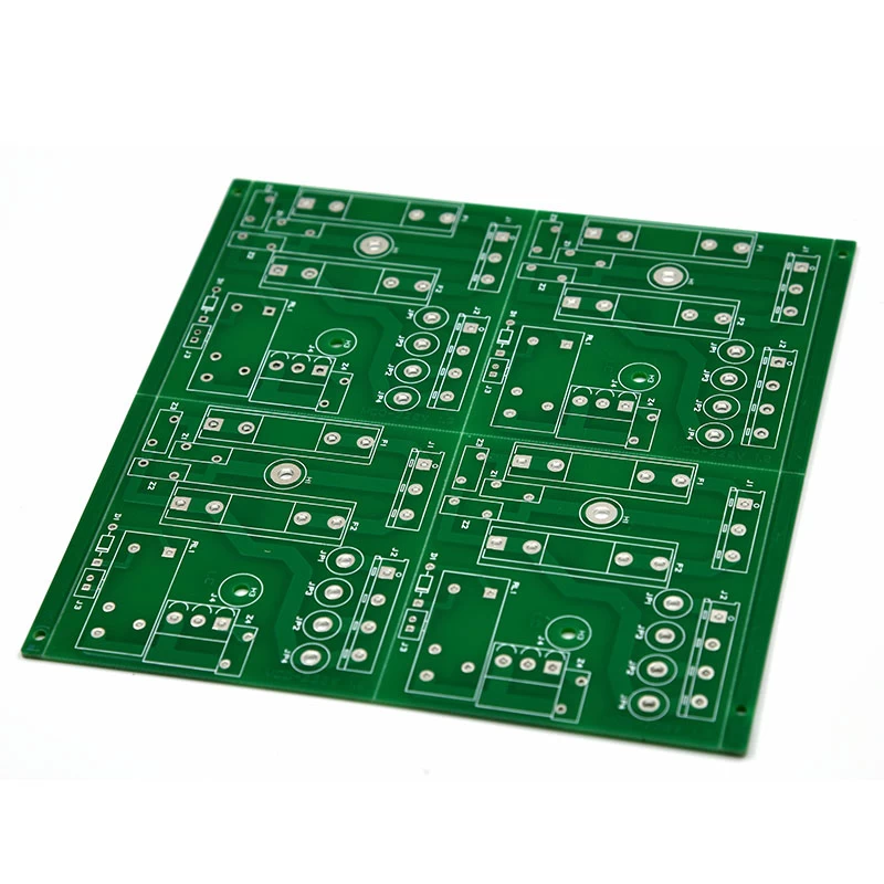
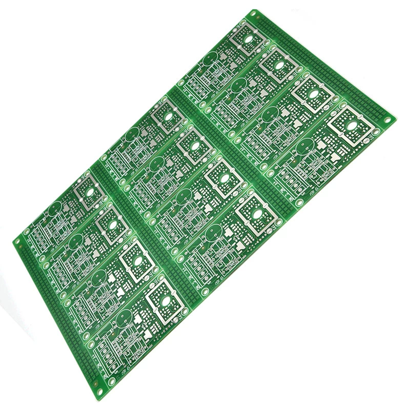
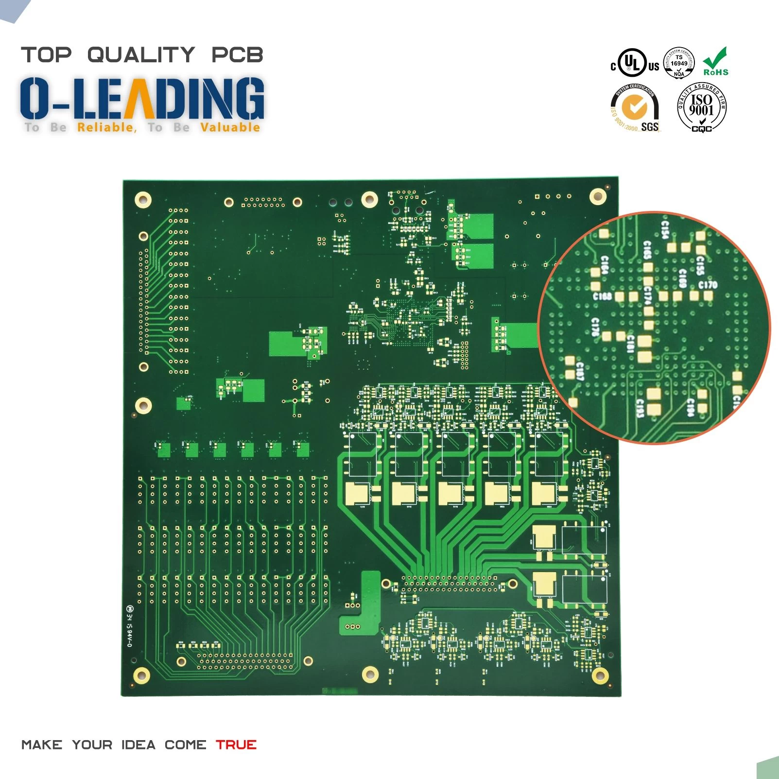
What should be paid attention to when PCB proofing?
Then, when laying out, what are the general points that should be paid attention to in order to make the documents you draw valid in line with the general PCB processing factory rules, so as not to cause unnecessary extra expenses for the enterprise?
The article summarizes the seven rules that PCB layout generally follows:
Thermal Management manufacturer china
One
Outer circuit design rules:
(1) Welding ring (Ring ring): The welding ring of the PTH (copper-plated hole) hole must be 8 mils larger than the single side of the drill hole, that is, the diameter must be 16 mils larger than the drill hole. The weld ring of the Via hole must be larger than the drilled one side. Large 8 mil, the diameter must be 16 mils larger than the hole. In any case, whether it is through hole PAD or Via, the inner diameter must be greater than 12 mil and the outer diameter must be greater than 28 mil. This is very important!
(2) The line width and line spacing must be greater than or equal to 4 mils, and the distance between the holes and the holes should not be less than 8 mils.
(3) The outer layer of the etched word line width is greater than or equal to 10 mils. Note that the word is etched instead of silk screen.
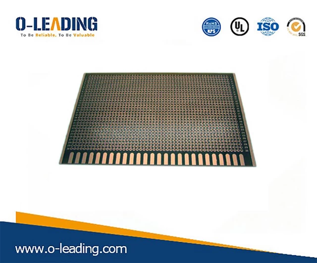
(4) The circuit layer is designed with a grid of plates (plated with copper in a grid shape), and the rectangle of the grid space is greater than or equal to 10*10 mil, that is, the line spacing should not be less than 10 mils when the copper is set.
The grid line width is greater than or equal to 8 mil. When laying a large area of copper, many materials are recommended to be meshed.
Printed circuit boards supplier
Firstly, it is possible to prevent the adhesive of the substrate of the PCB board and the copper foil from being generated during the dip soldering or heating, and the heat is not easily removed, thereby causing the copper foil to expand and fall off;
Second, more important is the grid-like paving of its thermal performance, high-frequency conductivity performance is much better than the solid paving of the whole block.
However, some siege lions believe that the advantages of grid-plated copper cannot be compromised in terms of heat dissipation. In consideration of local heating and PCB deformation, the net heat dissipation effect and the integrity of the PCB should be used as conditions. Grid copper.
The advantage of this copper-plated copper is that the surface temperature is somewhat improved, but it is still within the limits of commercial or industrial standards, and the damage to the components is limited.
However, if the direct result of the bending of the PCB is the occurrence of a virtual solder joint, it may directly lead to the fault of the line. The result of comparison is that the damage is small, and the real heat dissipation effect should be the best.
In practical applications, the copper in the middle layer is rarely grid-like, that is, the uneven force caused by temperature is not as obvious as the surface layer, and the solid copper with better heat dissipation effect is basically adopted.
(5) The distance between the NPTH hole and the copper is greater than or equal to 20 mils.
(6) The board formed by the seesaw (milling cutter), the distance of the copper from the forming line is 16 mil or more, so when laying, the distance of the trace from the frame should not be less than 16 mil. For the same reason, when slotting, the distance from copper should be 16 or more.
(7) The die-formed board has a distance of 20 mils from the molding line. If the board you are drawing may be mass-produced in the future, in order to save costs, it may be required to open the mold, so it must be foreseen when designing.
(8) V-CUT (generally draw a line in the Bottom Mask and Top Mask layers, preferably mark the V-CUT here), the board should be designed according to the thickness of the board;
[1] The plate thickness is 1.6 mm, and the distance of copper from the V-CUT line is greater than or equal to 0.8 mm (32 mil);
[2] The plate thickness is 1.2 mm, and the distance of copper from the V-CUT line is greater than or equal to 0.7 mm (28 mil);
[3] The thickness of the plate is 0.8mm-1.0mm, and the distance of copper from the V-CUT line is greater than or equal to 0.6mm (24mil);
[4] The plate thickness is 0.8 mm or less, and the distance of copper from the V-CUT line is greater than or equal to 0.5 mm (mil);
[5] Gold hand board, the distance of copper from the V-CUT line is greater than or equal to 1.2mm (mil).
Note: Do not set such a small spacing when assembling the board, as large as possible.
Two
Inner line design rules:
(1) Welding ring (Ring ring): The welding ring of the PTH hole must be 8 mils larger than the single side of the hole, that is, the diameter must be 16 mils larger than the hole. The welding ring of the Via hole must be 8 mils larger than the single side of the hole. 16 mils larger than the borehole. (2) Line width, line spacing must be greater than or equal to 4 mils.
(3) The inner layer has an etched word line width of 10 mils or more.
(4) The distance between the NPTH hole and the copper is greater than or equal to 20 mils.
(5) The board formed by the seesaw (milling cutter), the distance of copper from the forming line is greater than or equal to 30 mil (generally 40 mil).
(6) The inner layer of the non-weld ring PTH drilled to the copper foil is kept at least 10 mil (four-layer board), and the six-layer board is at least 11 mil.
(7) When the line width is less than or equal to 6 mil lines, and there is a hole in the pad, a teardrop must be added between the line and the pad.
(8) The isolation area between the two large copper faces is 12 mil or more.
(9) Heat dissipation PAD (plum pad), the distance from the edge of the drill hole to the inner circle is greater than or equal to 8 mil (ie Ring ring), the distance from the inner circle to the outer circle is greater than or equal to 8 mil, and the width of the opening is greater than or equal to 8 mil. Generally there are four openings. At least two openings are required.
Three
Drilling design rules
(1) The PCB board factory in principle designs the "8" shaped hole into a slot (annular hole). Therefore, it is recommended to make a ring as much as possible in the layout. There is no such function. You can put more than N circles and stack as many mistakes as possible.
In this way, the final ring groove will not appear "dog teeth", and the board factory will not break the drill bit because of your slot!
(2) The minimum mechanical drilling aperture is 0.25mm (10mil), and the general aperture design is greater than or equal to 0.3mm (12mil).
If it is smaller than this or just 0.25mm, the people in the board factory will definitely find you. why? [You can find the answer you want in (5)]
(3) The minimum slot diameter is 0.25mm (10mil), and the general aperture design is greater than or equal to 0.3mm (12mil). [same (2)]
(4) The general practice is that only the mechanical drilling unit is mm; the rest of the units are mil. The habit of drawing is that in addition to the library, the size is in mm, the rest is in mil units, and the mil unit is small, which is convenient.
(5) Laser drilling (laser) aperture is generally 4 mil (0.1 mm) -8 mil (0.2 mm). This technique is only used for boards with more than 6 layers and very dense.
For example, the mobile phone motherboard, of course, the price will definitely increase by one N level.
More important is the minimum processing factor of the PCB:
One to three-stage blind buried holes, laser (laser) drilling is 4 mils (0.10 mm) minimum, minimum line width is 4 mils (0.10 mm), and minimum gap is 4 mils (0.10 mm).
Buried holes, as the name suggests, are buried in the middle of the slab, but they are only used as guides. Blind holes, one that is exposed to the outside and hidden inside, are usually only used as general guides.
The laser (laser) drilling, the penetration thickness is less than or equal to 4.5 mil, but the round hole is punched out. So don't think about using the laser drilling (laser) process to get through the PAD. Via is hard to use. So be careful when placing the PAD, don't forget the 0.25mm limit.
Four
Text design principles:
The line width is 6 mils or more, the text is 32 mils higher, and the line width of the text box is 6 mils or more.
Fives
Hole copper and copper design principles
(1) The board of general finished copper 1OZ (35um), the hole copper is 0.7mil (18um).
(2) The general finished copper 2OZ (70um) board, hole copper 0.7mil (18um) - 1.4mil (35um).
Six
Soldering protection design principle
(1) The solder resist is 3 mils larger than the pad.
(2) The soldering distance line (copper skin) is greater than or equal to 3 mils.
(3) The green oil bridge is ≥ 4 mil, which is the gap (dam) between the solder joints of the IC pins.
(4) The BGA position window and cover line are greater than or equal to 2 mils, and the green oil bridge is designed. If the distance is not enough, the skylight window is made.
(5) The gold finger part of the gold finger board must be solder-proof open, including fake fingers.
(6)The wire diameter of the solder resist type is ≥8mi, and the word height is ≥32mil.


