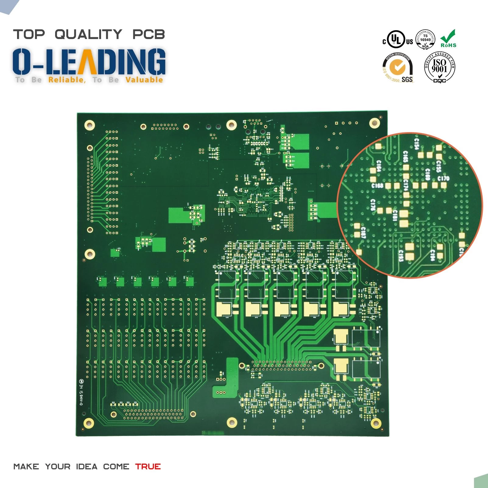
Seven good habits of PCB engineers
In the eyes of some people, the PCB layout engineer's work will be a bit boring, tens of thousands of wires every day against the board, a variety of packages, repeating the work of pulling the wire...
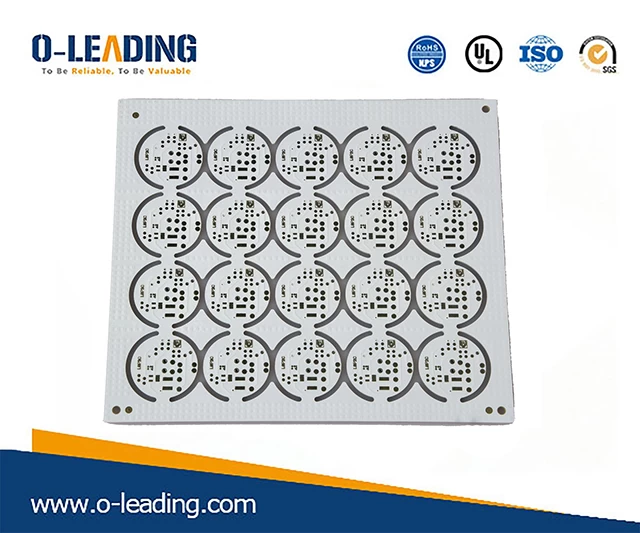
Halogen Free manufacturer china
In fact, it is not as simple as it seems. Designers must make trade-offs between various design rules, taking into account performance, process, cost and other aspects, but also pay attention to the layout of the board is reasonable and tidy.
As an excellent PCB layout engineer, good work habits will make your design more reasonable, better performance and easier to produce.
Here are 7 good habits of PCB layout engineers. Let's see if you have a few!
1 Learn the design rules
In fact, not only advanced PCB design software needs to set wiring rules, but some simple and easy-to-use PCB tools can also be set. After all, the human brain is not a machine, and it is inevitable that there will be negligence and mistakes.
So put some easy to ignore problems into the rules, let the computer help us check, try to avoid making some low-level mistakes.
In addition, the perfect rule setting can better regulate the work behind. The so-called sharpening of the knife does not mistakenly cut the woodworker. The more complicated the scale of the board, the more important the importance of the rule setting.
2 Perform DRC (Design Rules Check) as much as possible
Although it takes only a short time to run the DRC function on the PCB software, in a more complex design environment, as long as you perform checks during the design process, you can save a lot of time. This is a good habit to keep. Every cabling decision is critical, and you can always remind you of the most important cabling by performing a DRC.
3 draw a schematic
Many engineers feel that the layout work is more important. The schematic diagram is for the purpose of generating a netlist for PCB inspection. In fact, the schematic diagram will be more important in the subsequent circuit debugging process.
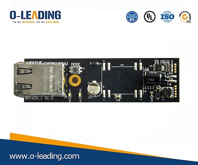
IC Substrate manufacturer china
Whether it's finding a problem or communicating with a colleague, the schematic is more intuitive and convenient. In addition, develop the habit of making annotations in the schematic diagram, and mark the problems that should be noticed when the various parts of the circuit are laid out on the schematic diagram, which is a good reminder to yourself or to others.
The hierarchical schematic diagram divides the circuits of different modules with different functions into different pages, so that the workload can be significantly reduced whether it is read or reused.
4 Optimize PCB layout
The anxious engineer draws the schematic diagram, and after importing the netlist into the PCB, he can't wait to put the device in place and start pulling the wire. In fact, a good PCB layout can make your wire drawing work easier and make your PCB work better.
Each board will have a signal path. The PCB layout should also follow this signal path as much as possible so that the signal can be transmitted smoothly on the board. People don't like to go through the maze, and the signal is the same. If the schematic is designed according to the module, the PCB is the same.
The board can be divided into several areas according to different functional modules. The analog numbers are separated, the power signals are separated, the heating device and the susceptible device are separated, the larger device is not too close to the board edge, pay attention to the shielding of the RF signal, etc. It takes a minute to optimize the layout of the PCB. Save more time when pulling the cable.

5 more for others to consider
When designing the PCB, consider as many end users as possible.
For example, if you are designing a development board, you should consider placing more silkscreen information when designing the PCB, so it will be more convenient when you use it. You don't have to go back and forth to find the schematic or find support from the designer.
If you are designing a mass-produced product, you should consider more of the problems encountered on the production line. The same type of device should be in the same direction, the device spacing is appropriate, the process side width of the board, and so on.
The earlier these issues are considered, the less the design will be affected, and the amount of work and the number of boards that will be supported later. It seems that the time spent on design has increased, actually reducing the amount of work that follows.
In the case that the board space signal allows, try to place more test points and improve the testability of the board, so that more time can be saved in the subsequent debugging stage, and more ideas can be provided for finding problems.
6 Repeated communication with customers
As an excellent PCB layout engineer, you must learn to communicate effectively with your customers.
Some important issues in Layout are best communicated with the customer repeatedly, such as the confirmation of the package.
Especially the position of the positive and negative poles, the triode, and the structural connector will directly affect the installation and positioning of the late board.
7 details determine success or failure
PCB design is a meticulous job that requires care and patience.
The mistakes often made by newcomers who are just beginning to design are some details. The device pins are wrong, the device package is wrong, the pin sequence is reversed, and so on, some can be solved by flying lines, and some may make a board directly become waste.
When you draw the package, check it again. Before you cast the board, print the package and compare it with the actual device. Look at it more. It is not obsessive-compulsive to check it again. It is just to avoid these low-level mistakes that are easy to make.
Otherwise, the design of the good-looking board, covered with flying lines, is far from excellent.
Good work habits will benefit you a lot.


