


PCB wave soldering process and mold process size requirements
Use shielding die wave soldering process technology
Because traditional wave soldering technology cannot handle the soldering of fine-pitch, high-density SMD components on the soldering surface, a new method has emerged: the use of a shielding die to shield the SMD components to achieve wave soldering of the soldering surface plug-in leads.
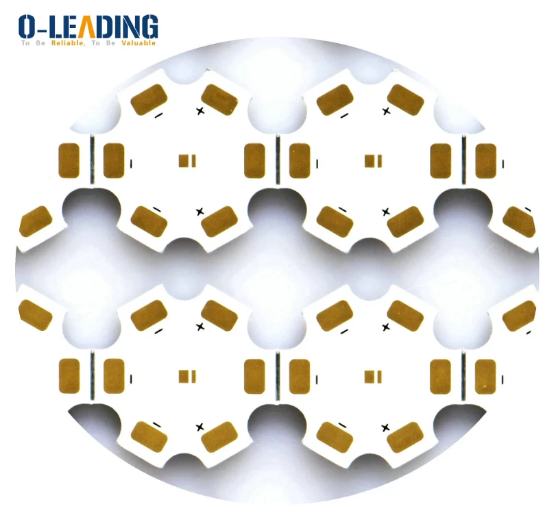
SMD Led Light pcb Factory for Led Grow Light
1. The advantages of using shielded die wave soldering technology
1) Realize double-sided mixed PCB wave soldering production, which can greatly improve the production efficiency of double-sided mixed PCB and avoid the problem of poor quality consistency in manual soldering.
2) Reduce the preparation time for pasting solder mask, improve production efficiency and reduce production costs.
3) The output is equivalent to traditional wave soldering.
2. Shielding mold material
1) The mold must be anti-static. Common materials are: aluminum alloy, synthetic stone, fiberboard. In order to avoid the wave soldering sensor not sensing when using synthetic stone, it is recommended not to use black synthetic stone.
2) Make the thickness of the mold base material. According to the thickness of the components on the back side of the machine disc, a base material with a thickness of 5mm to 8mm is selected to make a mold.
Shenzhen PCBA one stop service SMD assembly PCB
Mold process size requirements
1) Dimensions of the mold: The length and width of the mold are respectively equal to the length and width of the PCB plus the width of the 60mm carrier side and the mold width must be ≦350mm. When the PCB width is less than 140mm, you can consider placing two PCBs in a mold for welding.
2) The process side is 8mm away from the edge, and the other two sides are close to the edge with 10mm wide and 10mm high bakelite strips to increase the strength of the mold and reduce the deformation of the mold.
3) Each reinforcement bar must be fixed with screws, and the distance between the screw and the screw is less than 150mm.
electronic oem 4 layer printed circuit board assembly sensor pcba factory
4) After the mold is made, it is necessary to install the press buckle (fix the PCB on the mold) around and within 100mm, and pay attention to the following points:
① Do not touch the parts after one revolution;
②Does not affect DIP plug-in;
③It can stabilize the PCB in the mold.
5) The four corners of the mold should be chamfered with R5.
6) When the PCBA on the mold passes through the tin furnace, some parts will rise due to the impact of the tin wave. Therefore, the pressing method is used to solve some parts that are easy to float.
The main methods currently used:
①Pressed pieces of metal iron block;
②Install pressing parts on the mold;
③Producing anti-floating high-pressure parts fixtures.