


PCB complete processing
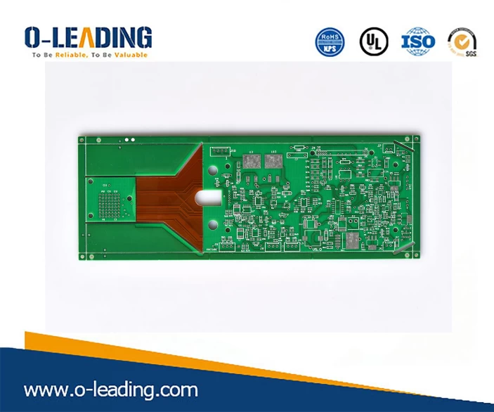
Multiple Flex-Rigid Board factory
The first step: the raw materials of the PCB board factory are generally 1020mm×1020mm and 1020mm×1220mm specifications. If the size of the board or the board is not suitable, a lot of raw materials will be produced in the PCB production process. The PCB board factory will add the price of some waste edges to your board, so that your PCB board price is more expensive; if the board size is well designed, the size of the board or board is n equal to the raw material. Then, the utilization rate of raw materials is the highest, and the PCB board factory is also good to open the material. With the same raw material size, the most boards are made, and the price of the board is the cheapest. We cut the purchased CCL into the size we need, called the material.
Cutting equipment: (cut the large board into small boards) The earliest copper clad board is a dielectric layer with copper on both sides.
Step 2: Typesetting
The third step: Film imports and modifies the graphic files provided by the customer through software, and finally outputs the graphics on the film. Film is film or silver salt photographic film, also known as film. Made of PC/PP/PET/PVC material. Now generally refers to film, but also refers to the film in the printing plate.
Flex printed circuit board supplier
Step 4: Exposure
A layer of photosensitive liquid is applied to the surface of the copper clad plate. After 80 degrees of temperature test, it is baked and dried on the PCB board, and then exposed to the ultraviolet exposure machine to remove the film.
Step 5: Etching a single etching process can be broken down into the following steps:
Plate、Developing Cylinder 1、Developing Cylinder 2、 Washing 1、Washing 2、Washing 3、Etching 1、Etching 2、Washing 1、Washing 2、Washing 3、Fading Film 1、Fading Film 2、Washing 1、Washing 2、Washing 3、drying、receiving board
Why is the etching method inside and outside the PCB different:
Inner layer: development → etching → peeling the outer layer: development → two copper tin plating → peeling → etching → peeling tin Why do this? Is the outer layer etched more than the process? The inner layer generally has a large line width and a large line spacing, so the Ring ring is sufficient;
Outer layer: The general line is dense and the space is not enough. Therefore, it is necessary to find a way to achieve the purpose of making the line in insufficient space. The ability to erode can reach 1~2mil ring, but the acid etching needs about 5mil, so it is necessary to use tin to protect the required line first.
Step 6: Drill the machine to drill holes in the PCB according to the size and coordinates of the vias in the file. If it is made of non-metallic holes, the circuit board factory must use dry film or do two diamonds or plug rubber, no matter how it is done, it will increase the cost of the board. So if you don't ask for it, the board factory will usually make metal holes for you.
Step 7: The copper sinking copper is a layer of chemical thin copper on the non-conductive substrate (hole wall) and copper surface.
Step 8: Green oil, characters
last step: when testing the sample, test the impedance and connectivity of all traces.