


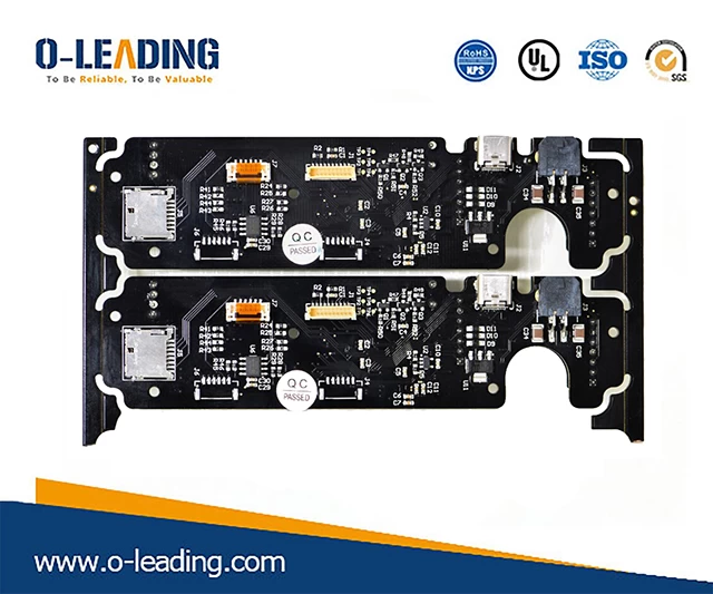
PCB circuit board is blocked by holes. Why?
The Via hole is used to connect the wires to each other. The development of the electronics industry also promotes the development of PCBs. It also places higher demands on the manufacturing process and surface mount technology of printed boards. The Via hole plugging process came into being, and the following requirements should be met:
(1) There is copper in the via hole, and the solder resist can be plugged;
(2) There must be tin-lead in the via hole, which has a certain thickness requirement (4 micrometers), and no soldering ink is allowed to enter the hole, resulting in the inclusion of tin beads in the hole;
(3) The via hole must have a solder-proof ink plug hole, which is opaque, and must not have tin ring, solder ball and leveling requirements.
With the development of electronic products in the direction of “light, thin, short and small”, PCBs are also developing at a high density and high difficulty. Therefore, a large number of SMT and BGA PCBs are present, and customers require plugging holes when mounting components. Five roles:
(1) Preventing the short circuit of the solder from passing through the component surface when the PCB is over-wave soldering; especially when we place the via hole on the BGA pad, we must first make the plug hole and then gold-plated to facilitate the BGA soldering.
(2) avoiding flux remaining in the via hole;
(3) After the surface mounting and component assembly of the electronics factory is completed, the PCB is vacuumed on the test machine to form a negative pressure:
(4) Preventing the surface solder paste from flowing into the hole to cause solder joints and affecting the mounting;
(5) Preventing the soldering of the solder balls during the wave soldering, causing a short circuit.
Implementation of conductive hole plug hole process
For surface mount boards, especially for BGA and IC mounting, the via hole must be flat, the bump is plus or minus 1 mil, and the edge of the via hole is not red tinned; the via hole is hidden in the tin, in order to reach the customer. The requirements of the via hole plug hole process can be described as various, the process is particularly long, the process control is difficult, and often there is oil drop during the hot air leveling and green oil solder resistance test; the problem of oil explosion after curing occurs. According to the actual conditions of production, the various plugging processes of PCB are summarized, and some comparisons and explanations are made in the process, advantages and disadvantages:
Note: The working principle of hot air leveling is to remove the excess solder on the surface of the printed circuit board and the holes by using hot air. The remaining solder is evenly covered on the pads and the unresisted solder lines and surface package points, which is the way of processing the surface of the printed circuit board. one.
I. Hot air leveling and plugging process
The process flow is: plate surface soldering→HAL→plug hole→curing. The non-plugging process is used for production. After the hot air is leveled, the aluminum plate or the ink-blocking net is used to complete the via hole of all the plugs required by the customer. The plug ink can be made of photosensitive ink or thermosetting ink. In the case of ensuring the same color of the wet film, the plug ink preferably uses the same ink as the surface of the board. This process can ensure that the through hole does not drop oil after the hot air is leveled, but it is easy to cause the plug hole ink to pollute the surface and uneven. Customers are prone to soldering during placement (especially within the BGA). So many customers do not accept this method.
Second, the hot air leveling front plug hole process
2.1 Using aluminum sheets to plug holes, solidify, and grind the board for pattern transfer
This process uses a CNC drilling machine to drill the aluminum sheet of the plug hole to make a screen plate, to make the plug hole, to ensure the plug hole is full, the plug ink plug hole ink, and the thermosetting ink can also be used, and the characteristics must be hard. The resin shrinks little and has good adhesion to the pore walls. The process flow is: pre-treatment → plug hole → grinding plate → pattern transfer → etching → surface solder mask
This method can ensure that the through hole of the through hole is flat, the hot air leveling will not have quality problems such as oil explosion and oil drop on the hole, but this process requires thickening copper once, so that the copper thickness of the hole wall reaches the customer's standard. Therefore, the whole plate copper plating is very demanding, and the performance of the plate grinding machine is also very high, ensuring that the resin on the copper surface is completely removed, the copper surface is clean and not polluted. Many PCB factories do not have a one-time thick copper process, and the performance of the equipment does not meet the requirements, resulting in the use of this process in the PCB factory is not much.
2.2 Direct screen printing surface soldering after plugging with aluminum
This process uses a CNC drilling machine to drill the aluminum sheet of the plug hole to make a screen. It is installed on the screen printing machine to carry the plug hole. After the plug hole is completed, it should not be parked for more than 30 minutes. The screen is directly screen printed with 36T screen. The process is: pre-treatment - plug hole - silk screen - pre-bake - exposure - development - curing
This process can ensure that the through-hole cover oil is good, the plug hole is flat, the wet film color is consistent, the hot air leveling can ensure that the conductive hole is not tinned, the tin beads are not hidden in the hole, but it is easy to cause the ink in the hole after curing. The pad causes poor solderability; after the hot air is leveled, the edge of the via hole is foamed and oil is lost. It is difficult to use this process for production control, and the process engineer must use special procedures and parameters to ensure plug quality.
2.3 Aluminum plate plug hole, development, pre-curing, after the plate is polished.
Using a CNC drilling machine, the aluminum piece required to be plugged is drilled to make a screen, which is installed on the shift screen printing machine to make the plug hole, the plug hole must be full, the two sides protrude better, and then the solidified plate is processed for the surface treatment. The process is: pre-treatment - plug hole - pre-bake - development - pre-cure - plate surface solder resist
Since the process uses plug hole curing to ensure that the HAL does not drop oil and oil after the HAL, after the HAL, the tin in the via hole and the tin on the via hole are difficult to completely solve, so many customers do not receive it.
2.4 Plate surface soldering and plugging are completed at the same time.
This method uses a 36T (43T) screen, installed on the screen printing machine, using a pad or a nail bed, and plugs all the through holes while completing the board surface. The process flow is: pre-processing - silk screen - - Prebaking - exposure - development - curing.
The process time is short, the utilization rate of the equipment is high, the hole can be ensured that the hot air is not drained, and the via hole is not tinned. However, since the screen hole is used for plugging, a large amount of air is stored in the via hole, and when solidified, The air expands and breaks through the solder mask, causing voids and unevenness. The hot air leveling will have a small amount of conductive vias. At present, our company has carried out a large number of experiments, choose different types of ink and viscosity, adjust the pressure of silk screen, etc., basically solve the hole void and unevenness, has been mass-produced by this process.