PCB board dry area problem solving chapter 1
1. Why does the BGA position in the solder mask? What is the acceptance criteria?
Answer: First, the soldering plug hole is used to protect the service life of the via hole. Because the hole required for the BGA position is generally small, between 0.2 and 0.35mm, some syrup in the hole is not easy to be processed in the post process. It is dried or evaporated, and it is easy to leave any residue. If it is not plugged in the solder mask or the plug is not full, it will be processed in the later process such as: tin, gold, there will be residual foreign matter or tin beads, in the customer's paste When the component is heated at high temperature, foreign matter or solder balls in the hole will flow out and stick to the component, causing defects in the performance of the component, such as opening and shorting. BGA is located in the soldering pad hole A, must be full of B, no redness or false copper. C. Do not allow the plug to be too full. The bump is higher than the pad to be soldered next to it. Effect).
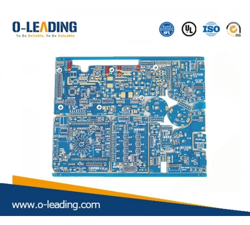
Double Side PCB manufacturer china
2. What is the difference between the countertop glass and the ordinary glass of the exposure machine? Why is the reflector of the exposure lamp uneven?
A: The tabletop glass of the exposure machine does not produce light refraction when the light is illuminated. If the reflector of the exposure lamp is smooth and smooth, then when the light is irradiated onto it, according to the principle of light, it forms only one reflected light onto the board to be exposed, if the pit is uneven, according to the light The principle, the light shining into the recess and the light shining on the convex part will form an infinite number of scattered light, forming irregular but uniform illumination onto the board to be exposed, improving the exposure effect.
3. What is side development? What are the quality consequences of the side development?
Answer: The bottom width area of the portion where the green oil is developed by the solder-proof window is called side development. When the side development is too large, it means that the green oil area which is in contact with the substrate or the copper skin is larger, and the dangling degree formed by it is larger, and the processing in the latter process is as follows: spray tin, sink tin When the side developing part such as Shen Jin is attacked by high temperature, pressure and some potions that are more aggressive to green oil, oil will be formed. If the IC part has a green oil bridge, when the customer installs the welding element, Will cause a bridge short circuit.
4. What is the poor soldering exposure? What kind of quality consequences does it cause?
Answer: After the solder mask process is processed, the pads of the post-process mounting components or the places to be soldered are exposed, which are caused by the light blocking film or the exposure energy and operation during the solder mask alignment/exposure process. The green oil covered by this part is exposed to the cross-linking reaction. During the development, the green oil in this part is not dissolved by the solution, and the outside or all of the part of the pad to be soldered is not exposed, which is called welding. Poor exposure. Poor exposure can result in failure to mount components, poor soldering, and severe open circuits.
5, the line, resistance welding, why should we deal with the grinding plate?
Answer: 1. The circuit board surface includes a foil-clad board substrate and a pre-plated copper substrate after metallization of the hole. In order to ensure the firm adhesion of the dry film and the substrate surface, the surface of the substrate is required to have no oxide layer, oil stain, fingerprint and other dirt, no drilling burr, no rough coating. In order to increase the contact area between the dry film and the surface of the substrate, the substrate is also required to have a microscopically rough surface. In order to meet the above two requirements, the substrate should be carefully treated before filming. The treatment methods can be summarized as mechanical cleaning and chemical cleaning.
2, the same soldering resistance is the same reason, before the solder mask is to remove some of the oxide layer, oil stains, fingerprints and other dirt on the board surface, in order to increase the contact area of the solder resist ink and the board surface and more secure, It is also required that the surface of the board has a microscopically rough surface (just like a tire that makes up the car, the tire must be ground to a rougher surface to better bond with the glue). If the plate is not processed before the soldering or soldering, the surface of the board to be coated or the solder resist to be printed has some oxide layer, oil stain, etc., which will directly separate the solder mask and the circuit film from the board surface. The separation is formed, and the film processed in this place in the subsequent process is peeled off and peeled off.
6. What is viscosity? What is the effect of solder mask ink viscosity on PCB production?
A: Viscosity - is a measure of stopping or resisting flow. The viscosity of solder mask ink has a considerable influence on the production of PCB. When the viscosity is too high, it is easy to cause no oil or sticky net. When the viscosity is too low, the fluidity of the ink on the surface will increase, which will easily cause oil to enter the hole. And a local sub-oil book. Relatively speaking, when the thickness of the outer layer of copper is thicker (≥1.5Z0), the viscosity of the ink should be controlled to be lower. If the viscosity is too high, the fluidity of the ink will decrease, and the bottom and corner of the line will be Will form no oil, no lines.
7. What are the similarities and differences between poor development and poor exposure?
Answer: The same point: a is the surface of the exposed copper/gold soldering after the solder mask. The cause of b is basically the same, the time, temperature, exposure time and energy of the baking sheet.
Different points: the area formed by poor exposure is large, the residual solder resist oil is from the outside to the inside, and the width and Baidu are relatively uniform. Most of them appear on the non-porous pad, mainly because the ink in this part is exposed to ultraviolet light. Irradiation of light. The remaining solder resist oil is only a layer of oil comparison book at the bottom. Its area is not large, but it forms a film state. This part of the ink is mainly due to different curing factors and forms with the surface layer ink. A layered shape that typically appears on a holed pad.
8. Why is there a bubble in the solder mask? How to prevent it?
Answer: (1) The solder resist oil is generally prepared by mixing the main agent of the ink + curing agent + thinner. When the ink is mixed and mixed, some air remains in the liquid. When the ink passes through the scraper and the wire. The nets are squeezed to each other and flow to the surface of the board. When a strong light or a relatively high temperature is encountered in a short time, the gas in the ink will rapidly evaporate as the inks flow toward each other, (2 ), the line spacing is too narrow, the line is too high, the solder resist ink can not be printed on the substrate during screen printing, so that there is air or moisture between the solder resist ink and the substrate, and the gas is heated and expanded to cause bubbles during curing and exposure. (3) The single line is mainly caused by the line being too high. When the blade is in contact with the line, the angle between the blade and the line is increased, so that the solder resist ink cannot be printed on the bottom of the line, and there is gas between the side of the line and the solder resist ink. When heated, a small bubble forms.
Prevention: a. The prepared ink is used for printing after a certain period of time. The printed board is also static for a certain period of time, so that the gas in the ink on the surface of the board gradually evaporates with the flow of the ink, and then it is taken. Bake at the temperature.
9. What is the resolution?
Answer: In the distance of 1mm, the line or spacing of the dry film resist can be formed. The resolution can also be expressed by the absolute size of the line or the spacing. The separation rate of the dry film and the thickness of the resist film. The thickness of the polyester film is related. The thicker the resist film layer is, the lower the resolution is. When the light is transmitted through the photographic plate and the polyester film film, the light scatters due to the scattering effect of the polyester film on the light. Serious, the lower the resolution.
10. What is dry film and etch and plating resistance?
Answer: Anti-etching: The dry film resist layer after photopolymerization should be resistant to the etching of ferric chloride etching solution, persulfate, etching solution, acid chlorine, copper etching solution, sulfuric acid-hydrogen peroxide etching solution. In the above etching solution, when the temperature is 50-55 ° C, the surface of the dry film should be free of hairiness, leakage, lifting and falling off. Plating resistance: In acid bright copper plating, fluoroborate common lead alloy, fluoroborate bright tin-lead alloy and various pre-plating treatment solutions of the above plating, the dry film resist after polymerization should have no surface hair. , plating, lifting and falling off.
11. Why should I vacuum when the exposure machine is exposed?
A: In the non-parallel light exposure operation (exposure machine with "dot" as the light source), the degree of vacuum is a major factor affecting the quality of exposure. Air is also a dielectric layer, if exposed in the board, film There is air between the pumping membranes, then the refraction of light will be produced, which will affect the effect of exposure. The vacuum is not only to prevent the refraction of light, but also to prevent the gap between the film and the board from expanding, and to ensure the alignment. / The quality of the exposure.
12. What are the advantages of pre-treatment with volcanic ash grinding? Disadvantages?
Answer: Advantages: a. The combination of abrasive pumice powder particles and nylon brush is tangential to the cotton cloth, which can remove all the dirt and reveal fresh and pure copper. b. It can form completely sanded, rough and uniform. , multi-peak surface, no arable trench; c, due to the relaxation of the nylon brush, the connection between the surface and the hole will not be damaged; d, due to the flexibility of the relatively soft nylon brush, can make up for The unevenness of the plate surface caused by the wear of the brush; e. Since the plate surface is uniform and has no grooves, the scattering of light during exposure is reduced, thereby improving the resolution of the imaging. Disadvantages: The deficiency is that the pumice powder is easy to damage the mechanical part of the equipment, the control of the particle size distribution of the pumice powder and the removal of the pumice powder residue on the substrate surface (especially in the hole).
13. What effect will the development point be too large or too small?
A: The correct development time is determined by the development point (the point at which the unexposed dry film is revealed from the printed board), and the development point must be maintained at a constant percentage of the total length of the development section. If the development point is too close to the exit of the developing section, the unpolymerized resist film is not sufficiently cleaned and developed, and the residue of the resist may remain on the board surface to cause development to be unclean. If the development point is too close to the entrance of the developing section, the polymerized dry film may become haired by being eroded by Na2C03 due to contact with the developer for a long time, and the film is removed and the gloss is lost to cause overdevelopment. Usually the development point is controlled within 40% - 60% of the total length of the developing section (35% - 55% of our company).
14. Why do you pre-bake the board before the character is printed?
Answer: Before the character printing, the pre-bake plate a is used to enhance the bonding force between the board and the character, and b enhances the hardness of the surface solder resist ink on the surface of the board, preventing the character printing or the post-processing process from easily causing the solder mask.
15. Why should the grinding of the pre-treatment grinding machine be swayed?
Answer: There is a certain distance between the brush and the needle. If there is no need to swing the plate directly, there will be many places that cannot be worn, resulting in uneven surface cleaning. Without swinging, a straight groove will be formed on the plate surface. Causes a broken line, and it is easy to break the hole and cause a tailing phenomenon without swinging the hole.
16. What is the role of the scraper on printing?
Answer: The angle of the scraper directly controls the amount of oil. The uniformity of the scraping surface directly affects the surface quality of the printing.
17. What is the effect of temperature and humidity in the soldering and wiring darkroom on PCB production?
Answer: When the temperature and humidity in the darkroom is too high or too low: 1. It will increase the garbage in the air. 2. It is easy to appear sticky film phenomenon in the opposite position. 3. It is easy to cause deformation of the film. 4. It is easy to cause oxidation of the board surface.
18, why not do soldering to develop points?
A: Because there are many variable factors in solder resist inks, first of all, there are many kinds of inks, and the properties of each ink are different. The thickness of each board ink during printing causes uniformity due to the influence of pressure, speed and viscosity. Different, not as dry film, the thickness is relatively uniform, and the solder resist ink is also affected by different baking time, temperature and exposure energy during the production process. Relatively speaking, the solder resist development point is difficult to guarantee for each piece. The effect of the board is the same, so the practical significance of solder mask to develop the point is not significant.
19. How is ghosting produced? How to prevent it?
A: Ghosts generally appear on the white board, and generally in the position of single-sided window opening, because the white material does not have the UV light blocking function, when the PCB is soldered and exposed, there will be some ultraviolet light in the unopened window. The edge of the PAD through the substrate to the window causes the green oil at the bottom of the green oil window to be exposed and not fully developed, forming ghosts. The ghosting of the yellow board is usually caused by the refraction or diffraction of ultraviolet light, which is generally more common in the gold finger position.

Prevention: 1. The window on the white board should be designed as a window with two sides as large as possible. 2. If the window is opened on one side, the back of the window opening is designed as large copper surface. 3. When the window is opened on one side and the back of the window is the substrate, the exposure energy of the substrate surface is 1-2 grids lower than that of the window surface.
20. What role does the solder mask ink play on the PCB?
A: Solder Mask Ink: It is a protective layer that is applied to substrates and lines where printed boards do not need to be soldered. The purpose is to prevent bridging between the lines during soldering, while providing a permanent electrical environment and a chemical, heat-resistant, and insulating protective layer, while providing an aesthetic appearance to the PCB. There are two major systems for solder mask ink: 1. Thermosetting epoxy ink, 2. Liquid photosensitive imaging ink.
21. What is the cause of excessive solder mask development?
Answer: 1. The exposure energy is too low, 2. The development speed is too slow, the pressure is too high, the concentration of the drug is too high, or the temperature of the developing cylinder is too high.
22, solder mask development of the board with green oil bridge, why the green oil bridge surface should be placed downwards?
A: Because the soldering green oil bridge generally has a small width (minimum 0.08mm), its attacking ability against developing water is relatively poor. When the green oil bridge is facing down, it is sprayed from the nozzle onto the board. The syrup has only one impact. If the syrup sprayed from the nozzle onto the board will bounce and hit the upper wall of the developing cylinder, it will form a new impact on the board, which will easily cause the broken green oil bridge. Therefore, the solder resist development green oil bridge deck should be placed downwards.
23. What are the reasons for green oil foaming?
Answer: There are: 1. Poor treatment before soldering resistance (speed too fast, too low temperature) causes the moisture in the hole to not completely dry, 2. There is gas in the bad hole of the plug hole, 3. The solder oil is too book, 4 If the character is not pre-baked according to the segment or the post-cure time is too long, the green oil becomes brittle. 5. The temperature of the processing equipment in the post-process is too high.

24. What are the regular items for testing solder mask inks?
Answer: 1. Hardness test (6H pencil), 2. Acid, alkali, solvent (10%) for 30 minutes at room temperature, 3. Adhesion (3M-600# gluon), 4. Resistance to immersion gold, immersion tin, spray Tin, 5, thermal shock resistance (288 ° C ± 5 ° C 10 seconds ± 1 second) and so on.
25. What are the different effects of the solder resist reversal screen printing machine and the front and rear, left and right shift screen printing machines in production?
Answer: When the screen printing machine moving forward and backward and the screen printing machine moving left and right are in production, if the holes on the board to be printed are vertically or in a row, it is easy to cause green oil to enter the hole, and the left and right displacement is also easy to pollute. On the left and right sides of the board, the printer is extremely inconvenient when taking the board, and the screen printing for diagonal movement is superior to the first two in terms of basic performance, if the holes on the board to be printed are vertical or one row The row is traversed, and the oblique diagonal displacement does not cause the holes to overlap and cause the oil to enter the hole.
26, why do dry film to develop?
A: Adjust to obtain a better development parameter speed by making a development point. If the development conditions are not determined at all, it is impossible to determine the different development conditions of each dry film, and it is not known how much the optimum developing ability of the developing machine used under certain parameter conditions. Usually the development point is controlled at 40% - 60%.
27. Why should I wash with alkali and pickle when the processor is being maintained?
Answer: The first use of alkaline washing is to clean the residual dirt and green oil of each cylinder. The acid washing is to absorb the alkaline substances remaining in the cylinder wall and nozzle and further clean.
28, how to improve the accuracy of solder mask alignment?
Answer: 1. Strengthen the actual operation skills of the training staff. 2. Use the ten-fold mirror to check the accuracy of the alignment when the position is in position. 3. Control the service life of the film. 4. Control the temperature inside the dark room within the required range. Prevent the deformation of the film, 4, design the alignment accuracy mark at the four corners of the board.
O-Leading Supply Chain CO., LTD
TEL: + 86-752-8457668
Fax: + 86-4008892163-239121
+ 86-2028819702-239121


