


Required knowledge about SMT, PCB, PCBA, DIP
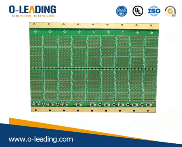
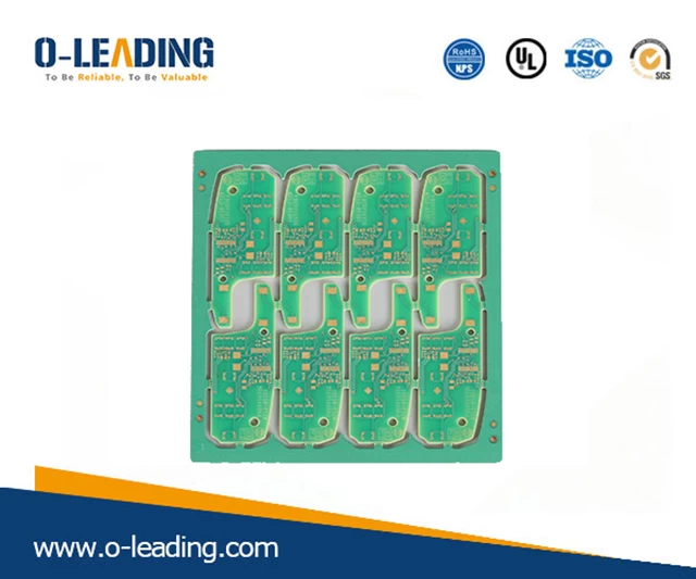
Printed circuit boards supplier
SMT features
The assembly density is high, the size of the electronic product is small, and the weight is light. The volume and weight of the chip components are only about 1/10 of that of the conventional plug-in components. After the SMT is generally used, the volume of the electronic product is reduced by 40% to 60%, and the weight is reduced by 60%. 80%.
High reliability and strong anti-vibration ability. The solder joint defect rate is low.
High frequency characteristics are good. Reduced electromagnetic and radio frequency interference.
Easy to automate and increase productivity. Reduce costs by 30% to 50%. Save materials, energy, equipment, manpower, time, etc.
Second, PCB is the most important of electronic components, no one. A conductive pattern which is formed on a dielectric material in a predetermined design to form a printed circuit, a printed component, or a combination of the two is generally referred to as a printed circuit. The conductive pattern that provides electrical connection between the components on the insulating substrate is called a printed circuit board (or printed circuit board), which is an important support for electronic components and can carry the carrier of the components.
PCB printed circuit board
We usually open a computer keyboard to see a soft film (flexible insulating substrate) printed with silver-white (silver paste) conductive patterns and figure-up graphics. Since the universal screen printing method obtains such a pattern, we call this printed wiring board a flexible silver paste printed circuit board. The printed circuit boards on the various computer motherboards, graphics cards, network cards, modems, sound cards and home appliances that we see in Computer City are different.
The substrate used is paper-based (usually used for single-sided) or glass-based (usually used for double-sided and multi-layer), pre-impregnated with phenolic or epoxy resin, and coated on one or both sides of the surface. Made. This kind of circuit board copper-clad sheet, we call it a rigid board. To make a printed circuit board, we call it a rigid printed circuit board.
Halogen free pcb factory china
Printed circuit graphics on one side We call a single-sided printed circuit board, printed circuit patterns on both sides, and printed circuit boards formed by double-sided interconnection through metallization of holes. We call it a double-sided board. If a double-sided inner layer, two single-sided outer layers or two double-sided inner layers and two single-sided outer printed circuit boards are used, the positioning system and the insulating bonding material are alternately The printed circuit boards in which the conductive patterns are interconnected according to the design requirements become four-layer and six-layer printed circuit boards, which are also called multi-layer printed circuit boards.
Third, PCBA is one of the basic components of electronic components. The whole process of PCB insertion through surface assembly technology (SMT) and DIP plug-in is called PCBA process. In fact, it is a patched PCB. One is a finished board and the other is a bare board.
PCBA can be understood as a finished circuit board, that is, after all the processes of the circuit board are completed, the PCBA can be counted. Due to the ever-increasing miniaturization and refinement of electronic products, most of the current boards use etch resists (film or coating), and after exposure and development, the boards are etched.
In the past, the perception of cleaning was not enough because the PCBA was not densely packed. It was also considered that the flux residue was non-conductive and benign and would not affect the electrical performance.
Today's electronic assemblies tend to be smaller, even smaller devices, or smaller pitches. Pins and pads are getting closer and closer. Today's gaps are getting smaller and smaller, and contaminants may get stuck in the gaps. This means that relatively small particles, if left between the two gaps, are also possible. A bad phenomenon that causes a short circuit.
Controlled impedance PCB supplier in china
In recent years, the electronic assembly industry has become more and more aware of the cleaning and the voices of cleaning. It is not only the requirements for products, but also the requirements for the environment and the protection of human health. Therefore, there are many cleaning equipment suppliers and solution providers, and cleaning has become one of the main contents of the technical exchange seminar in the electronic assembly industry.
DIP is one of the basic components of electronic components, called dual in-line package technology, which refers to integrated circuit chips packaged in dual-in-line form factor, which is also used in most small and medium-sized integrated circuits. Form, the number of pins is generally not more than 100.
DIP capacitor plug-in
The CPU chip of the DIP package technology has two rows of pins that need to be inserted into a chip socket having a DIP structure.
Of course, it can also be directly inserted on a circuit board having the same number of holes and geometric arrangement for soldering.
DIP packaging technology should be especially careful when plugging and unplugging from the chip socket to avoid damage to the pins.
Features include: multi-layer ceramic dual in-line DIP, single-layer ceramic dual in-line DIP, lead frame type DIP (including glass ceramic sealing type, plastic encapsulation structure, ceramic low-melting glass encapsulation type) and so on.
DIP plug-in welding is a very important process in the processing of pcba patch. The processing quality directly affects the function of pcba board, and its importance is very important. Then post-welding, because some components, according to the limitations of the process and materials, can not be welded by the wave soldering machine, can only be done by hand.
This also reflects the importance of DIP plug-ins in electronic components, only attention to detail, can be a hundred secrets.
In these four major electronic components, each has its own advantages, but complement each other, in order to form this series of production process, only the quality of the production products can be checked, so that a wide range of users and customers can appreciate our intentions.