What should I pay attention to when pcb proofing?
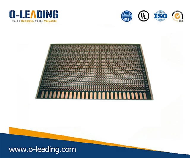
Printed circuit boards supplier
Then, when laying out, what are the general points that should be paid attention to in order to make the documents you draw valid in line with the general PCB processing factory rules, so as not to cause unnecessary extra expenses for the enterprise?
The article summarizes the seven rules that PCB layout generally follows:
Outer circuit design rules:
(1) Welding ring (Ring ring): The welding ring of the PTH (copper-plated hole) hole must be 8 mils larger than the single side of the drill hole, that is, the diameter must be 16 mils larger than the drill hole. The weld ring of the Via hole must be larger than the drilled one side. Large 8 mil, the diameter must be 16 mils larger than the hole. In any case, whether it is through hole PAD or Via, the inner diameter must be greater than 12 mil and the outer diameter must be greater than 28 mil. This is very important!
(2) The line width and line spacing must be greater than or equal to 4 mils, and the distance between the holes and the holes should not be less than 8 mils.
(3) The outer layer of the etched word line width is greater than or equal to 10 mils. Note that the word is etched instead of silk screen.
(4) The circuit layer is designed with a grid of plates (plated with copper in a grid shape), and the rectangle of the grid space is greater than or equal to 10*10 mil, that is, the line spacing should not be less than 10 mils when the copper is set.
The grid line width is greater than or equal to 8 mil. When laying a large area of copper, many materials are recommended to be meshed.
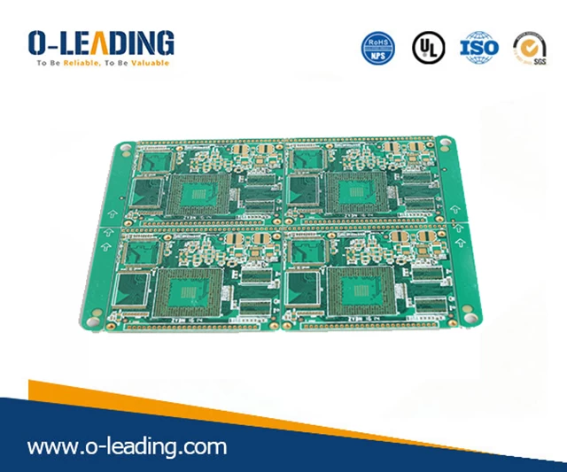
Multilayer PCB manufacturer in china
Firstly, it is possible to prevent the adhesive of the substrate of the PCB board and the copper foil from being generated during the dip soldering or heating, and the heat is not easily removed, thereby causing the copper foil to expand and fall off;
Second, more important is the grid-like paving of its thermal performance, high-frequency conductivity performance is much better than the solid paving of the whole block.
However, some siege lions believe that the advantages of grid-plated copper cannot be compromised in terms of heat dissipation. In consideration of local heating and PCB deformation, the net heat dissipation effect and the integrity of the PCB should be used as conditions. Grid copper.
The advantage of this copper-plated copper is that the surface temperature is somewhat improved, but it is still within the limits of commercial or industrial standards, and the damage to the components is limited.
However, if the direct result of the bending of the PCB is the occurrence of a virtual solder joint, it may directly lead to the fault of the line. The result of comparison is that the damage is small, and the real heat dissipation effect should be the best.
In practical applications, the copper in the middle layer is rarely grid-like, that is, the uneven force caused by temperature is not as obvious as the surface layer, and the solid copper with better heat dissipation effect is basically adopted.
(5) The distance between the NPTH hole and the copper is greater than or equal to 20 mils.
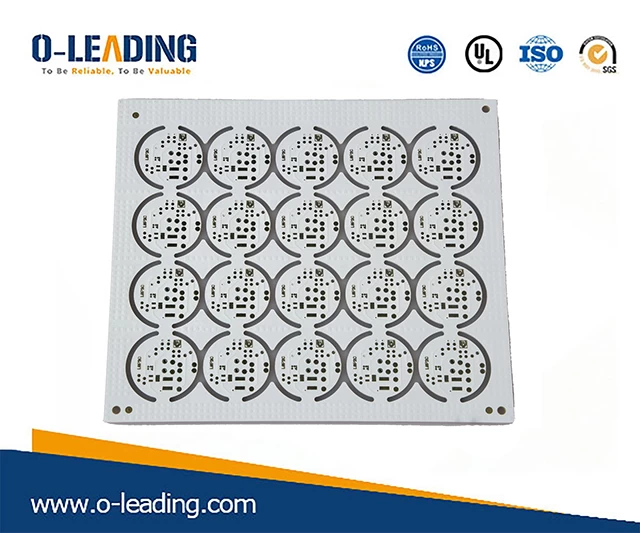
China Rigid-flexible pcb on sale
(6) The board formed by the seesaw (milling cutter), the distance of the copper from the forming line is 16 mil or more, so when laying, the distance of the trace from the frame should not be less than 16 mil. For the same reason, when slotting, the distance from copper should be 16 or more.
(7) The die-formed board has a distance of 20 mils from the molding line. If the board you are drawing may be mass-produced in the future, in order to save costs, it may be required to open the mold, so it must be foreseen when designing.
(8) V-CUT (generally draw a line in the Bottom Mask and Top Mask layers, preferably mark the V-CUT here), the board should be designed according to the thickness of the board;


