A brief introduction to the PCBA process
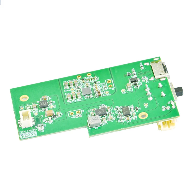
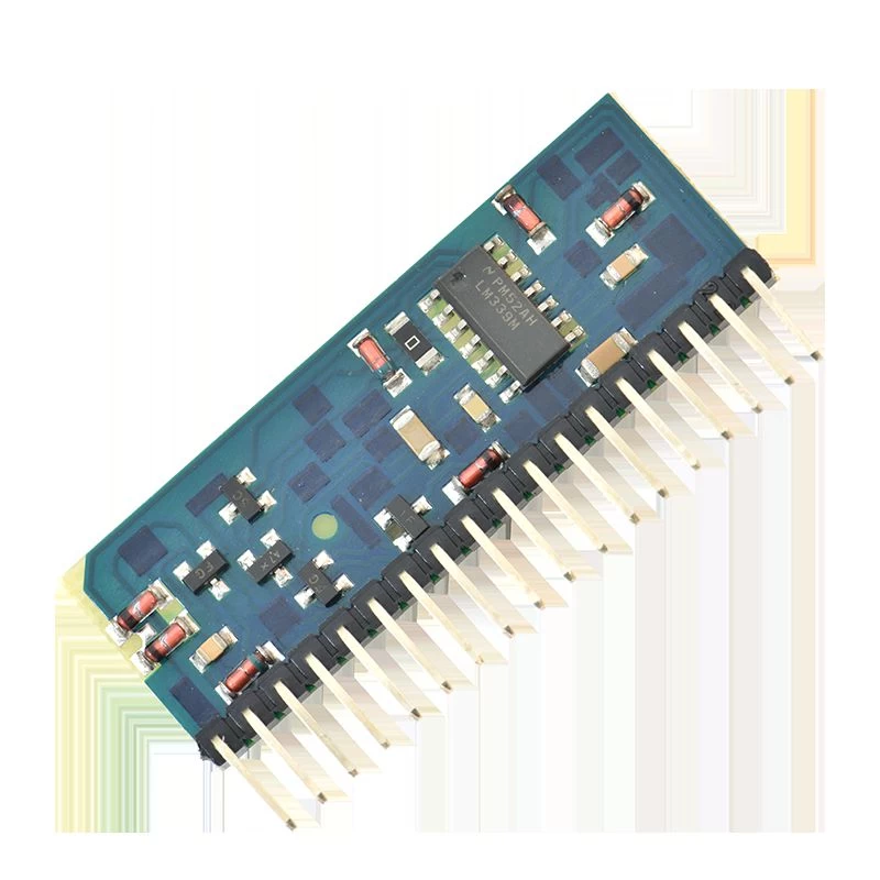
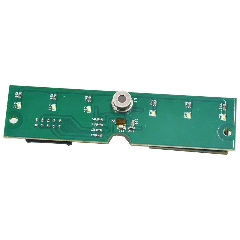
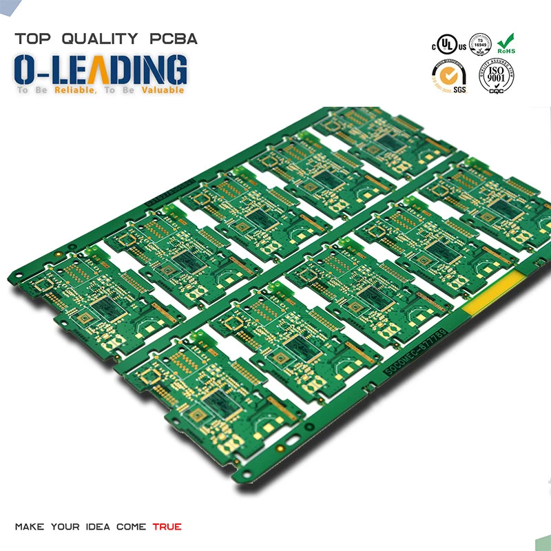
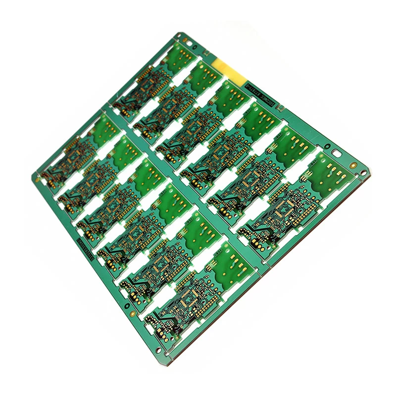
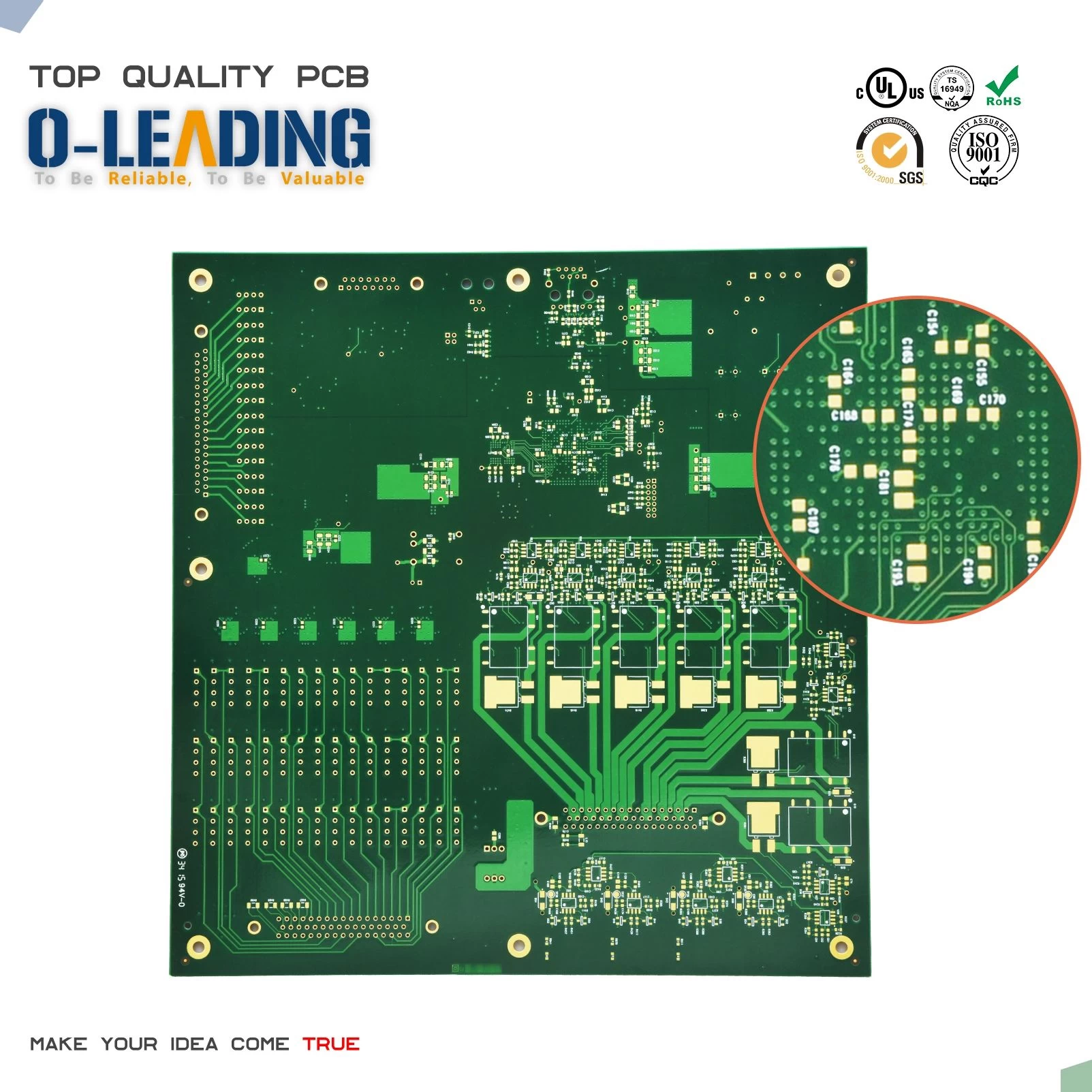
PCBA process involves carrier board, printing, patching, reflow soldering, plug-in, wave soldering, testing and quality inspection. See the following figure:
Different types of PCB boards have different process processes, and the differences are elaborated below in various cases.
1, single-sided SMT placement
The solder paste is added to the component pad, and after the solder paste of the bare PCB is printed, the relevant electronic components are reflow soldered and then reflow soldered.
2, single-sided DIP cartridge
The PCB board that needs to be plugged in is soldered by the production line workers after inserting the electronic components. After the soldering is fixed, the board can be washed by the foot, but the wave soldering production efficiency is low.
3, single-sided mixing
The PCB board is printed with solder paste, and the electronic components are mounted and fixed by reflow soldering. After the quality inspection is completed, DIP is inserted, and then wave soldering or manual soldering is performed. If there are fewer through-hole components, manual soldering is recommended. .
4, single-sided placement and cartridge mixing
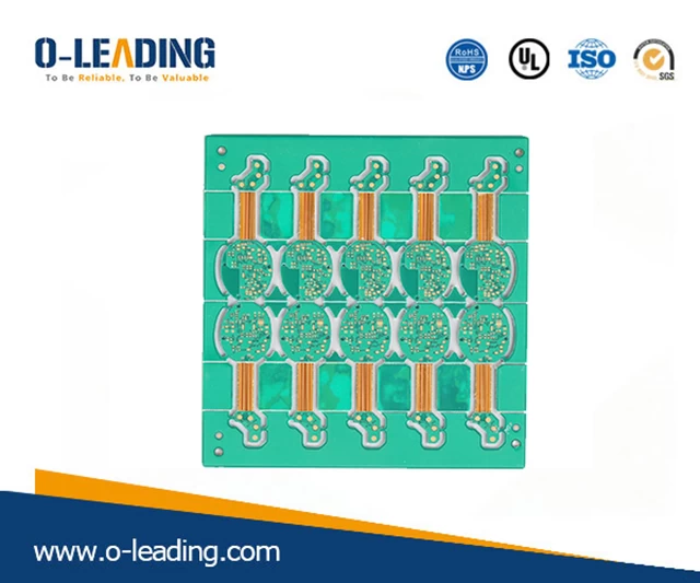
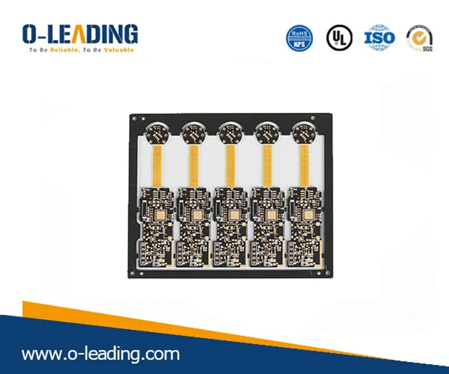
Some PCB boards are double-sided, one side is mounted, and the other side is inserted. The process of placement and insertion is the same as that of single-sided processing, but the PCB requires reflow and wave soldering.
5, double-sided SMT placement
In order to ensure the aesthetics and functionality of the PCB, some PCB board design engineers use a double-sided mounting method. Among them, the A side is arranged with IC components, and the B side is mounted with chip components. Make full use of PCB space to minimize PCB area.
6, double-sided mixing
Printed circuit boards supplier
The two methods are mixed in the following two ways. The first method is to assemble the PCBA three times for heating, the efficiency is low, and the pass rate of the wave soldering using the red glue process is low. The second method is suitable for the case where there are many double-sided SMD components and there are few THT components, and manual soldering is recommended. Wave soldering is recommended if there are many THT components.
The above content is only to simplify the PCBA assembly process of the printed circuit board, and to display the process in a graphic manner. However, as the PCBA assembly process and production process are gradually optimized, the failure rate is also continuously reduced, ensuring the production of high-quality finished products.
The solder joint quality of all electronic components described above determines the quality of the PCBA board. Therefore, when the relevant electronics manufacturers are looking for PCBA assembly and processing manufacturers, it is best to have a high level of experience and high processing equipment.

