


Analysis of the causes of PCB board deformation
The deformation of PCB board needs to be studied from several aspects such as material, structure, pattern distribution, processing process, etc. This paper will analyze and expound various reasons and improvement methods that may cause deformation.
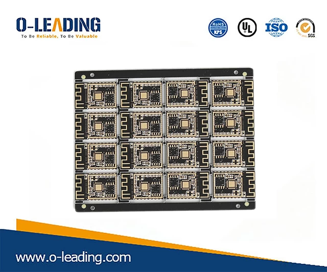
Multilayer PCB manufacturer in china
The uneven copper surface area on the board will deteriorate the board bend and the board curl.
Generally, a large area of copper foil is designed for grounding. Sometimes the Vcc layer is also designed with a large area of copper foil. When these large areas of copper foil are not evenly distributed on the same board. When it is on, it will cause the problem of uneven heat absorption and heat dissipation. The circuit board will of course also expand and contract. If the expansion and contraction cannot cause different stresses and deformation at the same time, the temperature of the board can be reached. At the upper end of the Tg value, the board begins to soften, causing permanent deformation.
The junctions(vias) of the various layers on the board limit the board's expansion and contraction.
Most of today's boards are multi-layer boards, and there are joints (vias) to the rivets between the layers. The joints are divided into through holes, blind holes and buried holes. Where there are joints, the board is limited. The effect of rising and contracting will indirectly cause the plate to bend and the plate to be warped.
Reasons for PCB board deformation:
(1) The weight of the circuit board itself will cause the board to be deformed
In general, the reflow furnace will use a chain to drive the advancement of the circuit board in the reflow furnace, that is, the two sides of the board are used as fulcrums to support the entire board. If the board has heavy parts on the board, or the size of the board is too large, It will show the phenomenon of the middle depression due to its own quantity, causing the plate to bend.
(2) The depth of the V-Cut and the connecting strip will affect the deformation of the panel.
Basically, V-Cut is the culprit in destroying the structure of the board. Because V-Cut cuts the groove on the original sheet, the V-Cut is prone to deformation.
2.1 Analysis of the deformation of the plate by pressing materials, structures and figures
The PCB board is formed by pressing a core board and a prepreg and an outer layer copper foil, wherein the core board and the copper foil are thermally deformed when pressed, and the amount of deformation depends on the coefficient of thermal expansion (CTE) of the two materials;
The coefficient of thermal expansion (CTE) of the copper foil is about 17×10-6;
The ordinary FR-4 substrate has a Z-direction CTE of (50-70) X10-6 at the Tg point;
Above TG point is (250~350) X10-6, X-direction CTE is similar to copper foil due to the presence of glass cloth.
Notes on TG points:
High Tg printed board When the temperature rises to a certain area, the substrate will change from "glass state" to "rubber state", and the temperature at this time is called the glass transition temperature (Tg) of the board. That is, Tg is the highest temperature (°C) at which the substrate remains rigid. That is to say, the ordinary PCB substrate material not only softens, deforms, melts, etc. at high temperatures, but also exhibits a sharp drop in mechanical and electrical properties.
Generally, the Tg plate is 130 degrees or more, the high Tg is generally greater than 170 degrees, and the medium Tg is greater than about 150 degrees.
A PCB printed board with a typical Tg ≥ 170 °C is called a high Tg printed board.
The Tg of the substrate is improved, and the characteristics such as heat resistance, moisture resistance, chemical resistance, and stability of the printed board are improved and improved. The higher the TG value, the better the temperature resistance of the sheet, especially in the lead-free process, the high Tg application is more.
High Tg refers to high heat resistance. With the rapid development of the electronics industry, especially the electronic products represented by computers, the development of high functionality and high multi-layer requires the higher heat resistance of PCB substrate materials as an important guarantee. The emergence and development of high-density mounting technology represented by SMT and CMT makes PCBs more and more inseparable from the high heat resistance of substrates in terms of small aperture, fine wiring and thinning.
Therefore, the difference between general FR-4 and high Tg FR-4 is that it is in the hot state, especially under heat absorption, the mechanical strength, dimensional stability, adhesion, water absorption and thermal decomposition of the material. There are differences in various conditions such as thermal expansion, and high Tg products are obviously better than ordinary PCB substrate materials.
The expansion of the core plate in which the inner layer pattern is made is different due to the difference in the pattern distribution and the thickness of the core sheet or the material characteristics. When the pattern distribution is different from the thickness or material characteristics of the core sheet, when the pattern distribution is relatively uniform, the material types are uniform, and Will produce deformation. When the PCB board laminate structure is asymmetrical or the pattern distribution is uneven, the CTE difference of different core boards will be large, and deformation will occur during the pressing process. The deformation mechanism can be explained by the following principle.
It is assumed that there are two kinds of core plates with different CTE differences, which are pressed together by a prepreg, wherein the C core of the A core plate is 1.5×10⁻⁵/°C, and the core plate length is 1000 mm. In the press-forming process as a prepreg of the bonding sheet, the two core sheets are bonded together by softening, flowing and filling the pattern, and curing in three stages.
Figure 1 shows the dynamic adhesion bottom curve of ordinary FR-4 resin at different heating rates. Under normal circumstances, the material starts to flow from about 90°C, and cross-linking cure starts at the point above TG. The prepreg is in a free state before curing. At this time, the core plate and the copper foil are in a state of being freely expanded after being heated, and the amount of deformation thereof can be obtained by the respective CTE and temperature change values.
Printed circuit boards supplier
Simulated press-fit conditions, the temperature is raised from 30°C to 180°C,
At this time, the deformation amounts of the two core plates are respectively
△LA=(180°C~30°C)x1.5x10-5m/°CX1000mm=2.25mm
△ LB = (180°C ~ 30°C) X2.5X10-5M /°CX1000mm = 3.75mm
At this time, since the semi-cure is still in a free state, the two core plates are long and short, and do not interfere with each other, and deformation has not yet occurred.
When pressed, it will be kept at high temperature for a period of time until the semi-curing is completely cured. At this time, the resin becomes solidified and cannot flow freely. The two core plates are combined. When the temperature drops, such as no interlayer resin binding, the core The plate will return to the original length and will not be deformed, but in fact, the two core plates are bonded by the cured resin at high temperature, and cannot shrink at will during the cooling process. The A core plate should shrink 3.75mm, actually When the shrinkage is greater than 2.25mm, it will be hindered by the A core plate. In order to achieve the balance between the two core plates, the B core plate cannot shrink to 3.75mm, and the A core plate shrinks more than 2.25mm, so that the whole plate is directed to the B core. The direction of the board changes, as shown in Figure 2.
Deformation during compression of different CTE core plates
According to the above analysis, the laminated structure and material type of the PCB have been uniformly distributed, which directly affects the CTE difference between different core plates and copper foils. The difference in shrinkage during the pressing process will pass through the solidification of the prepreg. The process is retained and eventually forms a deformation of the PCB board.
2.2 Deformation caused during PCB processing
The causes of deformation of the PCB board process are very complicated and can be divided into two stresses: thermal stress and mechanical stress. The thermal stress is mainly generated during the pressing process, and the mechanical stress mainly occurs during the stacking, handling and baking of the plates. The following is a brief discussion in the order of the process.
CCL material: CCL is double-sided, symmetrical structure, no pattern, copper foil and glass cloth CTE are almost the same, so there is almost no deformation caused by different CTE during the pressing process. However, the size of the CCL press is large, and there is a temperature difference in different areas of the hot plate, which may cause slight differences in the curing speed and degree of the resin in different regions during the pressing process, and the dynamic viscosity at different heating rates also has a large difference, so it also occurs. Local stress due to differences in the curing process. Generally, this stress will maintain equilibrium after pressing, but will gradually release deformation during future processing.
Press-fit: The PCB press-fitting process is the main process for generating thermal stress. The deformation due to different materials or structures is shown in the previous section. Similar to the clad copper clad, it also produces local stress caused by the difference in the curing process. Due to thicker thickness, various pattern distribution, and more prepreg, the thermal stress is more difficult to eliminate than the clad laminate. The stress existing in the PCB is released in subsequent processes such as drilling, contouring or grilling, resulting in deformation of the panel.
Soldering, character and other baking processes: Since the solder resist inks cannot be stacked on each other when cured, the PCB boards are placed on the shelf and cured by a baking sheet. The soldering temperature is about 150°C, just above the Tg point of the medium and low Tg materials, Tg Above the point, the resin is in a high elastic state, and the plate is easily deformed under the action of its own weight or strong wind of the oven.
Hot air solder leveling: The normal temperature of the hot plate solder is 225°C~ 265°C, the time is 3S-6S. The hot air temperature is 280 °C~ 300 °C. When the solder is leveled, the plate is fed into the tin furnace from room temperature, and then subjected to room temperature post-treatment water washing within two minutes after the furnace is discharged. The entire hot air solder leveling process is a quenching and quenching process. Due to the different material of the circuit board and the uneven structure, thermal stress will inevitably occur during the hot and cold process, resulting in microscopic strain and overall deformation.
Storage: The storage of the PCB in the semi-finished stage is generally inserted in the shelf. The loose adjustment of the shelf is not suitable, or the stacking of the board during storage will cause mechanical deformation of the panel. Especially for thin plates below 2.0mm, the impact is even more serious.
In addition to the above factors, there are many factors that affect the deformation of the PCB.