


What is PCB? Are you really understanding the PCB?
In the next few pages, we will discuss the composition of the PCB, including some terminology, a brief assembly method, and an introduction to the PCB design process.
What’s a PCB?
Printed circuit board (PCB) is one of the most common names, and can also be called "printed wiring boards" or "printed wiring cards". Before the PCB appeared, the circuit was made up of point-to-point wiring. The reliability of this method is very low, because as the circuit ages, the breakage of the line can cause an open or short circuit of the line node.
Winding technology is a major advancement in circuit technology that enhances the durability and replaceability of the line by winding small diameter wires around the posts at the joint.
As the electronics industry moves from vacuum tubes and relays to silicon semiconductors and integrated circuits, the size and price of electronic components are also declining. Electronic products are appearing more and more frequently in the consumer sector, prompting manufacturers to look for smaller and more cost-effective solutions. So, the PCB was born.
ComposiTIon (composition)
The PCB looks like a multi-layered cake or lasagna - a layer of different materials in the production, pressed together by heat and adhesive.
Start with the middle layer.
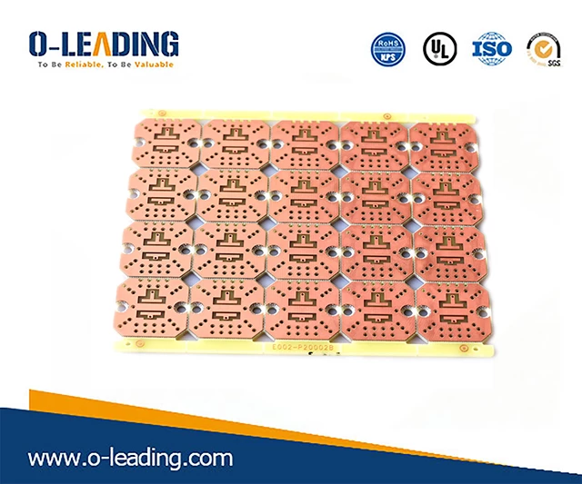
Prototype PCB Assembly company china
FR4
The substrate of the PCB is generally glass fiber. In most cases, the fiberglass substrate of a PCB is generally referred to as the "FR4" material. The solid material "FR4" gives the hardness and thickness of the PCB. In addition to the FR4 substrate, there are flexible circuit boards produced on flexible high-temperature plastics (polyimide or the like) and the like.
You may find PCBs of different thicknesses; however, the thickness of SparkFun's products is mostly 1.6mm (0.063' ‘). Some products also use other thicknesses, such as LilyPad and Arudino Pro Micro boards with a thickness of 0.8mm.
Cheap PCBs and hole plates (pictured above) are made of epoxy or phenolic materials and lack the durability of FR4, but they are much cheaper. When soldering things on such boards, you will smell a lot of odor. This type of substrate is often used in very low-end consumer products. Phenolic substances have a low thermal decomposition temperature, and the long welding time causes decomposition and carbonization, and gives off an unpleasant taste.
Copper
The following is a very thin copper foil layer that is pressed into the substrate by heat and adhesive during production. On the double-sided board, the copper foil is pressed to the front and back sides of the substrate. In some low-cost applications, copper foil may only be pressed on one side of the substrate. When we refer to "double-panel" or "two-layer board", it means that there are two layers of copper foil on our lasagna. Of course, in different PCB designs, the number of copper foil layers may be as small as 1 layer or more than 16 layers.
The thickness of the copper layer is relatively large and is measured in weight. It is generally expressed by the uniform weight of one square foot of copper (oz). Most PCBs have a copper thickness of 1 oz, but some high-power PCBs may use 2 oz or 3 oz of copper. Convert ounces (oz) per square foot, which is about 35um or 1.4mil copper.
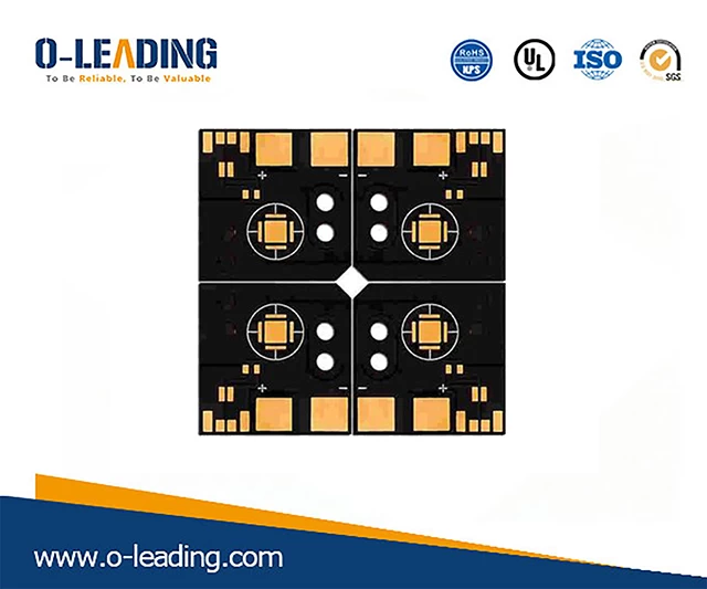
Power supply module manufacturer china
Soldermask
Above the copper layer is a solder mask. This layer makes the PCB look green (or SparkFun's red). The solder mask covers the traces on the copper layer to prevent traces on the PCB from coming into contact with other metals, solder or other conductive objects. The presence of a solder mask allows you to solder in the right place and prevent solder bridges.
In general, solder masks are all green, but almost all colors can be used for solder masking. Most of SparkFun's boards are red, but the IOIO board is white and the LilyPad board is purple.
Silkscreen
Above the solder mask, there is a white silk screen layer. Letters, numbers, and symbols are printed on the silkscreen of the PCB to facilitate assembly and guide you to better understand the design of the board. We often use the silkscreen symbol to indicate the function of certain pins or LEDs.
The most common color of the silk screen layer is white. Similarly, the silk screen layer can be made into almost any color. Black, gray, red and even yellow silk screens are not uncommon. However, it is rare to see a variety of silkscreen color on a single board.