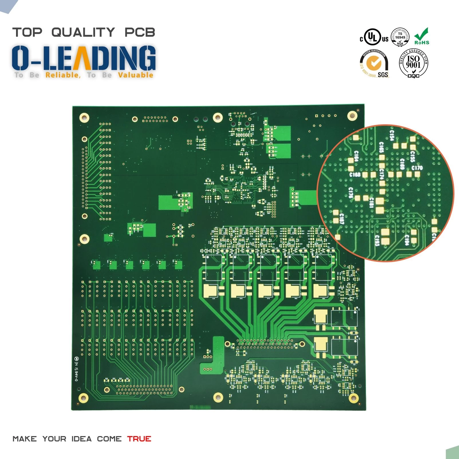
Static protection common problems and solutions
Multilayer PCB manufacturer in china
The scale of modern semiconductor devices is getting larger and larger, and the working voltage is getting lower and lower, which leads to the sensitivity of semiconductor devices to external electromagnetic disturbances. ESD has attracted more and more attention to the interference caused by circuits, damage to components, CMOS circuits and interface circuits. The ESD of electronic equipment has also begun to be written into national and international standards as an important part of electromagnetic compatibility testing.
Electrostatic causes and their harm
When static electricity is rubbed by two substances having different dielectric constants, the positive and negative polar charges are accumulated on two specific bodies. When two objects are in contact, one of them tends to attract electrons, and thus both form different charging potentials. In the case of the human body, the static electricity generated by the friction between the clothes and the skin is one of the main causes of human body charging.
When the static power source is in contact with other objects, there is a charge flow according to the mechanism of charge neutralization, which transfers enough power to offset the voltage. During the transmission of high-speed power, potential voltages, currents, and electromagnetic fields are generated. In severe cases, objects are destroyed. This is electrostatic discharge. It is defined in the national standard: Electrostatic discharge is a charge transfer caused by close proximity or direct contact of special electrostatic potentials (GB/T4365-1995), generally expressed by ESD. ESD can cause serious damage or malfunction of electronic equipment.
Electrostatic damage to the device is both dominant and recessive. The hidden damage was not visible at the time, but the device became more fragile and easily damaged under conditions of overpressure and high temperature.
The two main failure mechanisms of ESD are: the heat generated by the ESD current causes thermal failure of the device; the excessive voltage induced by ESD causes insulation breakdown. Both types of damage can occur simultaneously in one device, for example, insulation breakdown can excite large currents, which in turn leads to thermal failure.
In addition to the damage caused by the circuit, the electrostatic discharge is also very easy to cause interference to the electronic circuit. There are two ways in which electrostatic discharge can interfere with electronic circuits. One is conducted interference and the other is radiated interference.
The construction of digital products and their ESD problems
Nowadays, the functions of various digital products are getting stronger and stronger, while the boards are getting smaller and smaller, and the integration is getting higher and higher. More or less part of the interface is used for human-computer interaction, so there is an ESD problem of human body electrostatic discharge. The parts of general digital products that require ESD protection are: USB interface, HDMI interface, IEEE1394 interface, antenna interface, VGA interface, DVI interface, button circuit, SIM card, earphone and other various data transmission interfaces.
ESD can cause the product to work abnormally, crash, or even damage and cause other security problems. Therefore, before the product goes on the market, domestic or foreign inspection departments are required to test ESD and other surge surges. Among them, the contact discharge needs to reach ±8kV, and the air discharge needs to reach ±15kV, which puts high requirements on the design of ESD.
Controlled impedance PCB supplier in china
ESD problem solving and protection in digital products
3.1 Structural design of the product
If the released static electricity is regarded as a flood, then the main solution is similar to water control, which is “blocking” and “sparing”. If the product we design has an ideal housing that is airtight, there is no static electricity, so there is no static problem. However, the actual casing often has gaps in the cover, and many of them have metal decorative pieces, so be sure to pay attention.
First, use the "blocking" method. Try to increase the thickness of the casing, that is, increase the distance between the casing and the board, or increase the distance of the air gap of the casing by some equivalent methods, so as to avoid or greatly reduce the energy intensity of the ESD.
Through the improvement of the structure, the distance of the air gap between the outer casing and the internal circuit can be increased, so that the energy of the ESD is greatly reduced. As a rule of thumb, the 8kV ESD typically decays to zero after a distance of 4mm.
Second, using the "sparse" method, it can be sprayed on the inside of the casing with EMI paint. EMI paint is electrically conductive and can be thought of as a metallic shield that allows static electricity to be conducted on the housing. The housing is then connected to the ground of the PCB (Printed Circuit Board) to conduct static electricity away from the ground. In addition to preventing static electricity, the method of this treatment can effectively suppress EMI interference. If there is enough space, you can also protect the circuit with a metal shield, which is then connected to the GND of the PCB.
In short, there are many places to be aware of on the ESD design housing. The first step is to prevent the ESD from entering the inside of the housing and minimize the energy entering the housing. For the ESD entering the inside of the case, try to guide it away from GND and do not let it harm other parts of the circuit. Be careful when using metal decorations on the casing, as it is likely to bring unexpected results and requires special attention.
3.2 PCB design of the product
The PCB (Printed Circuit Board) of the current product is a high-density board, usually a 4-layer board. As the density increases, the trend is to use a 6-layer board, and its design always needs to consider the balance of performance and area. On the one hand, the larger the space, the more space can be placed on the components. At the same time, the wider the line width and the line spacing, the benefits for EMI, audio, ESD and other aspects. On the other hand, the compactness of digital product design is also a trend and need. Therefore, you need to find a balance point when designing.
Halogen free pcb factory china
As far as the ESD problem is concerned, there are many places to pay attention to in design, especially regarding the design of the GND wiring and the line spacing. In some products, there is a big problem with ESD, and there is always no reason. Through repeated research and experimentation, it is found to be a problem in PCB design. To this end, here is a summary of the points that should be noted in PCB design:
(1) The distance between the PCB board edge (including the via hole Via boundary) and other wirings should be greater than 0.3mm;
(2) The board edges of the PCB are preferably all surrounded by GND traces;
(3) The distance between GND and other wiring is kept at 0.2mm~0.3mm;
(4) The distance between Vbat and other wiring is kept between 0.2mm and 0.3mm;
(5) The distance between important lines such as Reset, Clock, etc. and other wirings should be greater than 0.3mm;
(6) The distance between the high-power line and the other wiring is kept at 0.2 mm to 0.3 mm;
(7) There should be as many vias (VIa) as possible between the GNDs of different layers;
(8) Avoid sharp corners in the final paving. Sharp corners should be as smooth as possible.
3.3 Product Circuit Design
In the design of the housing and PCB, after paying attention to the ESD problem, ESD will inevitably enter the internal circuit of the product, especially the following ports: USB interface, HDMI interface, IEEE1394 interface, antenna interface, VGA interface , DVI interface, button circuit, SIM card, earphones and other types of data transmission interfaces, these ports are likely to introduce static electricity from the human body into the internal circuit. Therefore, ESD protection devices need to be used in these ports.
The electrostatic protection devices used in the past are varistor and TVS devices, but the common disadvantages of these devices are that the response speed is too slow, the discharge voltage is not accurate enough, the interelectrode capacitance is large, the life is short, and the electrical performance is deteriorated due to multiple uses. . Therefore, the current "static suppressor" is commonly used in the industry to replace the conventional static protection device.
"Static suppressor" is a professional solution to the problem of static electricity. Its internal structure and working principle are more scientific and professional than other products. It is made of Polymer polymer material, and the internal diamond molecules are arranged in a regular discrete shape. When the electrostatic voltage exceeds the trigger voltage of the device, the internal molecules rapidly generate a tip-to-tip discharge, which discharges the static electricity to the ground in an instant. Its biggest feature is fast response (0.5 ns ~ 1 ns), very low interelectrode capacitance (0.05pf ~ 3pf), very small leakage current (1μA), very suitable for various interface protection.
Because the static suppressor has many advantages such as small volume (0603, 0402), non-polarity, fast reaction speed, etc., the proportion of using static suppressors as protective devices in the current design is increasing, so pay attention to the following points when using:
1. Place the device as close as possible to the port to be protected;
2. The connection to GND is as short as possible;
3. The area of the connected GND is as large as possible.
The problem with ESD is one of many important issues. There are different ways to avoid damage to the circuit in different electronic devices. Due to the small size and high density of digital products, there are unique features in the protection of ESD. Through a large number of static test experiments, it is proved that the design method of this paper can protect and improve a product that would have been dead after ±2kV discharge, and it can still work stably under the condition of ± 8kV electrostatic discharge, which plays a very good static electricity. Protective effect.
With the increasing use of electronic devices, ESD design is a key concern for every structural design engineer and electronic design engineer. By continuously summarizing and learning, ESD issues will no longer be a problem!


