


PCB failure analysis technology (1)
As a carrier of various components and a hub for circuit signal transmission, PCB has become the most important and critical part of electronic information products. The quality and reliability of the PCB determine the quality and reliability of the entire equipment. However, due to cost and technical reasons, a large number of failures have occurred during the production and application of PCBs.
For this kind of failure problem, we need to use some commonly used failure analysis techniques to ensure the quality and reliability of the PCB during the manufacturing process to a certain degree of assurance. Summarize the failure analysis techniques for reference.
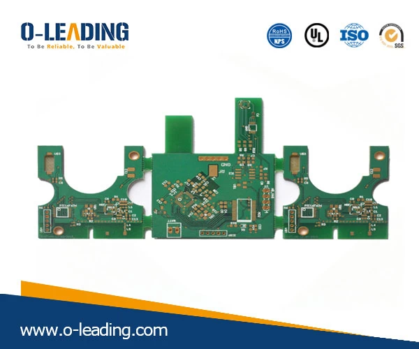
PCB for Telecommunication Device
1.Visual inspection
Visual inspection is to visually inspect or use some simple instruments, such as stereo microscopes, metallographic microscopes, and even magnifying glasses, to check the appearance of PCBs, to find the parts of failure and related physical evidence. The main functions are to locate failures and determine the failure mode of the PCB. The appearance inspection mainly checks the PCB's pollution, corrosion, the location of the explosion board, the circuit wiring and the regularity of the failure. If it is batch or individual, is it always concentrated in a certain area and so on. In addition, many PCB failures are discovered only after being assembled into a PCBA. Whether the failure is caused by the assembly process and the influence of the materials used in the process also requires careful inspection of the characteristics of the failure area.
2. X-ray fluoroscopy
For some parts that can not be inspected by appearance and the internal and other internal defects of the through holes of the PCB, the X-ray fluoroscopy system has to be used for inspection. X-ray fluoroscopy systems use different material thicknesses or different material densities to absorb X-rays or transmit light through different principles. This technique is more used to inspect the defects inside PCBA solder joints, the defects inside through holes and the positioning of defective solder joints for high-density packaged BGA or CSP devices. The current industrial X-ray fluoroscopy equipment can reach a resolution of less than one micron, and is changing from two-dimensional to three-dimensional imaging equipment. Even five-dimensional (5D) equipment has been used for packaging inspection. Light fluoroscopy systems are very expensive and rarely have practical applications in industry.
One-stop Turnkey PCB & PCBA Manufacturing
3. Slice analysis
Slice analysis is the process of obtaining the cross-section structure of the PCB through a series of methods and steps such as sampling, inlaying, slicing, polishing, corrosion, and observation. Through slice analysis, you can get rich information about the microstructure of the PCB (through-hole, plating, etc.) quality, which provides a good basis for the next quality improvement. However, this method is destructive. Once the sectioning is performed, the sample will be destroyed; meanwhile, the method requires high sample preparation, and the sample preparation takes a long time, which requires a trained technician to complete. For detailed slicing procedures, refer to the procedures specified in IPC's standard IPC-TM-650 2.1.1 and IPC-MS-810.
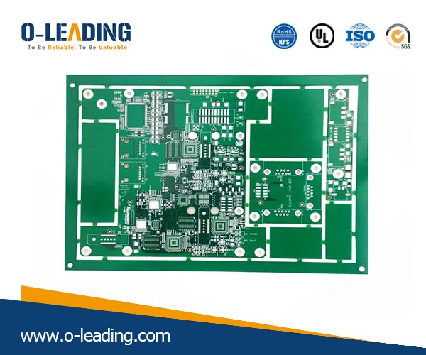
Impedance PCB manufacturer china
4. Scanning acoustic microscope
Currently, C mode ultrasonic scanning acoustic microscope is mainly used for electronic packaging or assembly analysis. It uses high frequency ultrasonic reflection on the discontinuous interface of materials to image the amplitude, phase and polarity changes. The scanning method is along the Z axis scans the information in the XY plane. Therefore, scanning acoustic microscopes can be used to detect various defects in components, materials, and PCBs and PCBAs, including cracks, delaminations, inclusions, and voids. If the frequency width of the scanning acoustics is sufficient, internal defects of the solder joints can also be detected directly. The typical scanning acoustic image is the red warning color to indicate the existence of defects. Because a large number of plastic-encapsulated components are used in the SMT process, a large number of moisture reflow sensitive problems occur during the process of converting lead to lead-free. That is, the hygroscopic plastic packaging device will crack internally or on the substrate when it is reflowed at a higher lead-free process temperature, and ordinary PCBs will often burst at the high temperature of the lead-free process. At this time, the scanning acoustic microscope highlights its special advantages in non-destructive testing of multilayer high-density PCBs. In general, the obvious bursting board can be detected only by visual inspection.