


Analysis of the three main reasons for PCB copper
The copper wire of the PCB is detached (also often referred to as beryllium copper). The PCB factory said that it is a laminate problem and requires its production plant to bear bad losses. There are several common reasons for copper in the PCB factory:

First, the PCB factory process factors:
1.Copper foil is excessively etched. The electrolytic copper foil used on the market is generally unilateral galvanized (commonly known as ash foil) and single-sided copper plating (commonly known as red foil). Common bismuth copper is generally galvanized copper of 70um or more. There are basically no batches of beryllium copper in foil, red foil and ash foil below 18um. When the customer circuit is designed to pass through the etched line, if the copper foil specification is changed and the etching parameters are not changed, the residence time of the copper foil in the etching solution is too long. Because zinc is originally a reactive metal, when the copper wire on the PCB is immersed in the etching solution for a long time, it will lead to excessive side etching of the line, causing some fine line backing zinc layer to be completely reacted and detached from the substrate. That is, the copper wire falls off. There is also a case where there is no problem with the PCB etching parameters, but the water is washed after etching, and the drying is poor, so that the copper wire is also surrounded by the etching liquid remaining on the surface of the PCB. If it is left untreated for a long time, excessive copper side etching will occur. Copper. This situation is generally manifested on the thin line, or in the wet weather, the same PCB will appear similarly bad, peeling off the copper line to see its contact with the base layer (the so-called rough surface) color has changed, Unlike the normal copper foil color, the original copper color is seen, and the peeling strength of the copper foil at the thick line is also normal.
2. Local collision occurs in the PCB process, and the copper wire is separated from the substrate by external mechanical force. This bad performance is poor positioning or directional, and the detached copper wire will have obvious distortion or scratches/impact marks in the same direction. Peel the copper wire on the bad copper strip to see the copper foil surface. You can see that the copper foil surface is normal in color, there will be no side erosion, and the copper foil peeling strength is normal.
3, PCB circuit design is unreasonable, the use of thick copper foil to design a thin line, will also cause excessive etching of the line and copper.
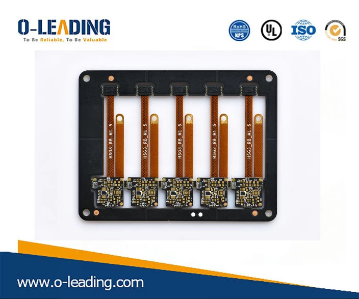
High quality PCB Assembly service
Second, the laminate process reasons:
Under normal circumstances, as long as the laminate is hot pressed for more than 30 minutes, the copper foil and the prepreg are basically completely combined, so the pressing generally does not affect the bonding force between the copper foil and the substrate in the laminate. However, in the process of stacking and stacking laminates, if PP is contaminated, or the damage of the copper foil surface is damaged, the bonding strength of the copper foil to the substrate after lamination may be insufficient, resulting in positioning (only for large plates). Words) or sporadic copper wire falling off, but the peeling strength of the copper foil near the test strip is not abnormal.
Third, the reasons for laminate raw materials:
1. It is mentioned above that ordinary electrolytic copper foil is galvanized or copper-plated products. If the peak of the wool foil is abnormal during production, or when galvanizing/copper plating, the plating crystal is poor, resulting in the copper foil itself. The peeling strength is not enough. When the defective foil pressed sheet is made into a PCB and is inserted into the electronics factory, the copper wire is broken by the external force. Such copper beryllium is peeled off by copper wire to see that the copper foil surface (ie, the contact surface with the substrate) does not have obvious side etching, but the peeling strength of the whole copper foil is very poor.
2. Poor adaptability of copper foil and resin: Some special performance laminates, such as HTg sheets, are different in resin system. The curing agent used is generally PN resin. The resin molecular chain structure is simple and solidified. The degree of cross-linking is low and it is necessary to match the copper foil with a special peak. When the laminate is produced, the copper foil is not matched with the resin system, so that the peeling strength of the metal foil of the sheet is insufficient, and the copper wire is not peeled off when the insert is inserted.