


The process from bare PCB to PCBA
What is PCB?
PCB (Printed Circuit Board) is an important electronic component, a support for electronic components, and a carrier for the electrical connection of electronic components. Because it is made using electronic printing, it is called a "printed" circuit board.
What is PCBA?
PCBA (Assembly of PCB) is the whole process of PCB blank board passing through SMT patch and then DIP plug-in, referred to as PCBA. PCBA is a commonly used writing method in China, and the standard writing method in Europe and America is PCB'A, which is added with a slash.
1. SMT placement process
SMT (Surface Mounted Technology) is a surface assembly technology (surface mount technology), which is the most popular technology and process in the electronic assembly industry.
Simply put, it is a type of surface mounting components without lead or short lead (abbreviated as SMC/SMD) on the surface of the printed circuit board (Printed Circuit Board, PCB) or other substrate surface, through reflow soldering Or dip soldering and other methods for welding and assembly of circuit assembly technology.
O-leading fast delivery Double Side Pcb Board Assembly Pcba Smt Service
What preparations need to be done before SMT placement?
1). There must be a MARK point on the PCB, also called a reference point, which is convenient for the placement of the placement machine, which is equivalent to the reference object;
2). To make steel mesh to help the deposition of solder paste, transfer the accurate amount of solder paste to the exact position on the empty PCB;
3). SMD programming, according to the provided BOM list, accurately position and place the components in the corresponding position of the PCB through programming.
After the above preparations are completed, SMT placement can be carried out.
First, the placement machine determines whether the board is in the correct direction according to the MARK point on the board. Then, the solder paste is brushed on the steel mesh, and the solder paste is deposited on the PCB pad through the steel mesh.
Next, the placement machine places the components on the corresponding position of the PCB according to the patch programming, and then reflows to make the components, solder paste and the circuit board effectively contact.
Finally, an automatic optical inspection is performed to check the components on the PCB board, including: virtual soldering, tin connection, device orientation, etc., but the functional inspection cannot be done because the board and plug-in components are not soldered.
It should be noted that some devices have positive and negative poles or pin sequences, so it is necessary to carry out incoming inspection to prevent patch errors, especially BGA packaged devices. If the direction is wrong, the subsequent disassembly and repair welding are compared Time-consuming and laborious.
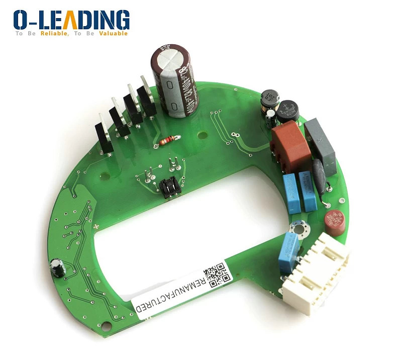
Industrial controller SMT assembly factory pcba Lidar IR Sensor board pcba(H08R6x)
2.the DIP plug-in process
DIP (Dual in-Iine Package) is the English abbreviation for dual in-line package. In fact, it is a device that can be soldered through the PCB board, commonly known as plug-in components.
What preparations need to be done before the DIP plug-in?
1). Prepare the furnace fixture and fix the PCB board to facilitate the transmission on the conveyor belt;
2). Need to modify the pins of the plug-in device with too long pins to a proper length;
3). Manpower is required to insert the plug-in device into the via hole of the corresponding PCB.
Next, a brief description of the DIP plug-in process: the DIP plug-in process is much simpler than the SMT placement process, but it requires human assistance to insert the plug-in components into the corresponding holes, and then pass the wave soldering machine, the plug-in device is perfectly welded On the PCB board.
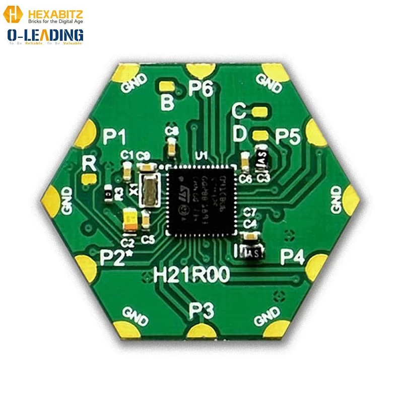
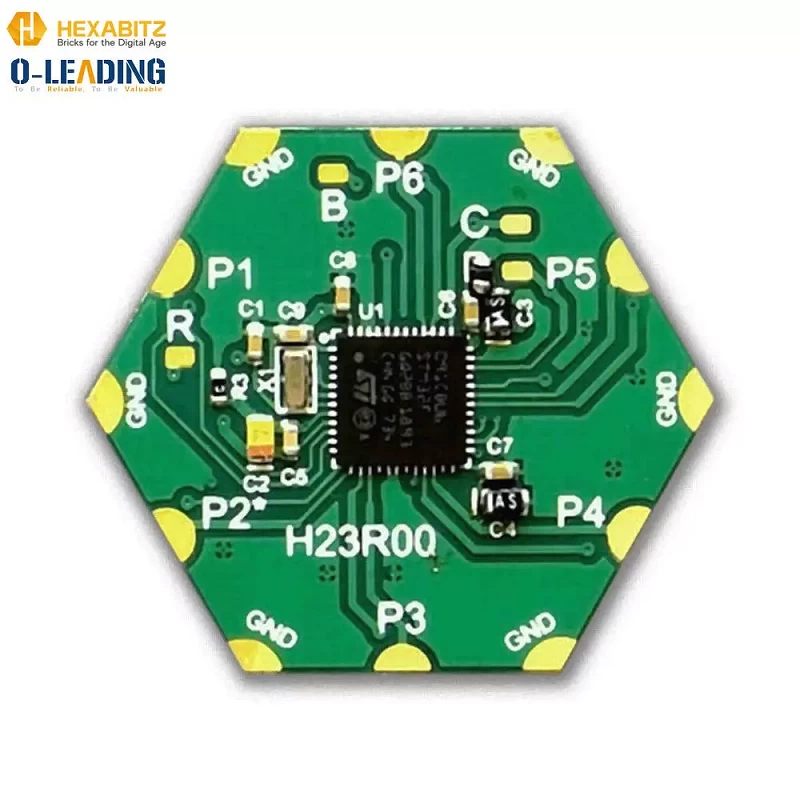
IMU and Digital Compass (H0BR4x) china pcb imu supplier
3. Perform functional test on the produced PCBA
The functional test of the PCBA produced can be divided into two steps:
The first step: human visual inspection of PCBA, preliminary screening out the problem board, such as: tin, virtual soldering, missing solder, etc. and visually visible errors, and then send the problem board to repair, the problem-free board will enter the second step.
Step 2: Check PCBA with the help of the test fixture, in fact, it is the power-on test function of the PCBA, and the corresponding test points of the PCBA are tested with the help of the test on the test fixture, such as: power on and off, relay pull-in, communication, etc. Whether the small modules on the board can work normally
After the above two-step screening, not only can the problem board be screened out, but also the problem board can be determined during the screening process, which reduces a certain amount of total work for subsequent repair of the problem board.
4. PCBA waterproof, dustproof and anti-corrosion treatment
Waterproof, dustproof and anticorrosive treatment is to spray paint or dip wax on PCBA.
Each company may have their own way of handling, some manual brushing of three anti-paint, some machines spraying three anti-paint, some of the dipping wax, of course, there is no treatment.