


Reasons for deformation of PCB board processing
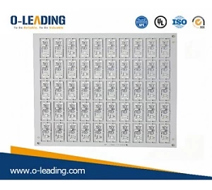
Single Side PCB manufacturer china
The causes of deformation of the PCB board process are very complicated and can be divided into two stresses: thermal stress and mechanical stress. The thermal stress is mainly generated during the pressing process, and the mechanical stress mainly occurs during the stacking, handling and baking of the plates. The following is a brief discussion in the order of the process.
CCL material: CCL is double-panel, symmetrical structure, no pattern, copper foil and glass cloth CTE are almost the same, so there is almost no deformation caused by different CTE during the pressing process. However, the size of the CCL press is large, and there is a temperature difference in different areas of the hot plate, which may cause slight differences in the curing speed and degree of the resin in different regions during the pressing process, and the dynamic viscosity at different heating rates also has a large difference, so it also occurs. Local stress due to differences in the curing process. Generally, this stress will maintain equilibrium after pressing, but will gradually release deformation during processing in the future.
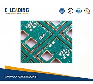
Ultra-thin PCB manufacturer china
Pressing: The PCB pressing process is the main process for generating thermal stress. The deformation due to different materials or structures is shown in the previous section. Similar to the clad copper clad, it also produces local stress caused by the difference in the curing process. Due to thicker thickness, various pattern distribution, and more prepreg, the thermal stress is more difficult to eliminate than the clad laminate. The stress existing in the PCB is released in the subsequent drilling, shape or grilling process, resulting in deformation of the plate.
Soldering, character and other baking processes: Since the solder resist inks cannot be stacked on each other when cured, the PCB board will be placed on the shelf and cured by a baking sheet. The soldering temperature is about 150 °C, just above the Tg point of the medium and low Tg material, Tg Above the point, the resin is in a high elastic state, and the plate is easily deformed under the action of its own weight or oven strong wind. ( Flexible PCB manufacturer china )
Hot air solder leveling: The normal temperature of the hot plate solder is 225 ° C ~ 265 ° C, the time is 3S-6S. The hot air temperature is 280 ° C ~ 300 ° C. When the solder is leveled, the plate is fed into the tin furnace from room temperature, and then subjected to room temperature post-treatment water washing within two minutes after the furnace is discharged. The entire hot air solder leveling process is a quenching and quenching process. Due to the different materials of the circuit board and the uneven structure, thermal stress will inevitably occur during the hot and cold process, resulting in microscopic strain and overall deformation.
Storage: The storage of the PCB in the semi-finished stage is generally inserted in the shelf. The loose adjustment of the shelf is not suitable, or the stacking of the board during storage will cause mechanical deformation of the panel. Especially for thin plates below 2.0mm, the impact is even more serious.