


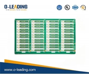
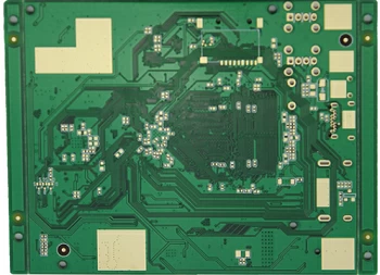
Quality requirements for solder joints on SMT chip PCB
High Tg PCB manufacturer china
1. Good appearance of PCB solder joints
(1) The solder joints on the pcb light board with good soldering quality should be clean, smooth and have a metallic luster. If there is dirt on the surface of the PCB and the residue after soldering, it may corrode the leads, pads and printed circuit boards of the components. If the moisture is absorbed, it may cause a partial short circuit or a leakage accident.
(2) There should be no burrs, voids, or tinning on the surface of the solder joint on the pcb light board. This not only affects the aesthetics of the smt patch solder joints, but also brings unexpected hazards, especially in high-voltage circuits, which may cause tip discharges, resulting in damage to electronic products.
(3) There is no abnormality on the surface of the solder joint on the pcb light board, otherwise the solder joint may be caused by the false solder joint or the false solder joint phenomenon, resulting in unreliable solder joints of the smt patch.
(4) Do not weld or touch weld to avoid short circuit events.
(5) The amount of solder should be suitable, not too much or too little, the surface of the smt patch solder joint is flat and has a semi-bow recess, the transition of the weldment is smooth, and the contact angle is small, so that it can be a qualified solder joint.
2, solder joints on pcb light board should have reliable electrical connection
There are two main functions of solder joints in soldering: one is to connect two or more components through solder; the other is to have good electrical characteristics.
Therefore, a solder joint must pass a certain amount of current stably and reliably, and there is not enough joint area and stable structure. Because the solder joint is not by pressure, but by the alloy layer firmly connected with the layer shape to achieve the purpose of electrical layer connection. (High Temperature PCB supplier china)
If only the solder is piled on the surface of the soldered component to form a solder joint, or only a small part of the alloy layer is formed, it may not be easy to find the solder joint in the test and initial work, but as the working conditions change.After the contact layer is oxidized, there may be a phenomenon of desoldering, and the circuit may be broken or simply not working. At this time, the appearance of the soldered circuit board is observed through the eyes, and the circuit is still connected, that is, it is not easy to check with the eyes, which is the most troublesome problem in the use of electronic equipment. Therefore solder joints must have a reliable electrical connection.