


What are the techniques for reducing the risk of pcb design?
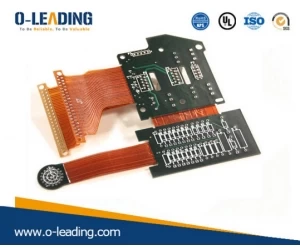
Flex printed circuit board supplier
In the PCB design process, if the possible risks can be predicted in advance and evaded in advance, the PCB design success rate will be greatly improved. Many companies will have a PCB design success rate when evaluating projects.
The key to improving the success rate of a board is the signal integrity design. At present, there are many product solutions for electronic system design, and chip manufacturers have already done it, including what chips are used, how to build peripheral circuits, and so on. Hardware engineers often do not need to consider the circuit principle in many cases, just need to make the PCB itself.
But it is in the PCB design process that many companies have encountered difficulties, either the PCB design is unstable or not working. For large enterprises, many chip manufacturers will provide technical support to guide PCB design. However, some SMEs have difficulty obtaining support in this regard. Therefore, we must find a way to complete it ourselves, so we have a lot of problems, we may need to play several editions and debug for a long time. In fact, if you understand the design method of the system, these can be avoided. Next, let's talk about three tips for reducing the risk of PCB design.
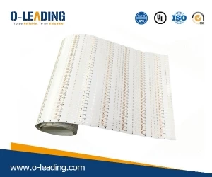
Golden Fingers PCB manufacturer china
In the first stage of the system planning, it is best to consider the signal integrity problem. The whole system is built like this. Can the signal be transmitted from one PCB to another? This is to be evaluated in the early stage, and it is not difficult to evaluate the problem. Knowing a little about signal integrity can be done with a simple software operation.
Second, in the PCB design process, using simulation software to evaluate the specific traces, to observe whether the signal quality can meet the requirements, the simulation process itself is very simple, the key is to understand the principle of signal integrity, and to guide.
Third, in the process of making PCB, it is necessary to carry out risk control. There are quite a few problems. At present, there is no way to solve the simulation software, and the designer must control it artificially. The key to this step is to understand where there are risks, what can be done to avoid risks, and what is needed is signal integrity. (Immersion Gold manufacturer china )
If you can grasp these three points in the PCB design process, the PCB design risk will be greatly reduced. The probability of error after playing back will be much smaller, and debugging will be relatively easy.