


Electromagnetic compatibility in printed circuit board development technology
ElectromagneticCompatibility refers to the ability of an electronic device to work in a coordinated and efficient manner in various electromagnetic environments. The purpose of the electromagnetic compatibility design is to enable the electronic device to suppress various external interferences, enable the electronic device to work normally in a specific electromagnetic environment, and at the same time reduce the electromagnetic interference of the electronic device itself to other electronic devices. Electromagnetic compatibility in printed circuit board design involves many factors.
Printed circuit board overall layout and device layout
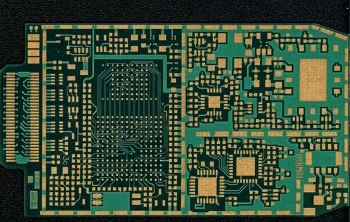
1. The success of a product, the first is to pay attention to the internal quality, the second is to take into account the overall aesthetics, both are more perfect to be considered the product is successful; on a PCB board, the layout of components needs to be balanced, sparse Ordered, can not be top-heavy or sinking, the number of vias should be as small as possible; the optimal shape of the board is rectangular. The aspect ratio is 3:2 or 4:3; the 4-layer board is 20dB lower than the double-panel noise. The 6-layer board is 10dB lower than the 4-layer board. The economical conditions allow the multi-layer board to be used as much as possible.
2. The circuit board is generally divided into analog circuit area, digital circuit area and power drive area, so the step board should be reasonably divided into three areas.
3. Devices generally choose devices with low power consumption and good stability, and use high-speed devices as little as possible.
4. The lines are exquisite: the conditional wide line is never made fine; the high pressure and high frequency lines should be smooth, no sharp chamfers, and corners should not be used. The ground wire should be as wide as possible. It is best to use a large area of ??copper, which has a considerable improvement on the grounding point problem.
5. The external clock is a high-frequency noise source. In addition to causing interference to the application system, it may also cause interference to the outside world, so that the electromagnetic compatibility test cannot reach the standard. In an application system that requires high system reliability, selecting a single-chip microcomputer with low frequency is one of the principles for reducing system noise.
6. In terms of device layout, as with other logic circuits, the related devices should be placed as close as possible to achieve better noise immunity. Clock generators, crystal oscillators, and CPU clock inputs are prone to noise, so be close to each other, especially under the crystal. Devices that are prone to noise, small current circuits, high-current circuits, etc. should be kept away from logic circuits as much as possible. If possible, it is important to make a separate board.
If you want to know more information about PCBs,please click the link Prototype PCB Assembly company china