


PCB structure and function introduction
We can think of copper foil as the blood vessels of adult bodies, to transport important blood, and to make PCBs active. Reinforcing materials can imagine the bones of adult bodies, which are used to support and strengthen PCBs without softening down; Resin can be imagined as the muscles of the human body and is the main component of the PCB.
The purpose, characteristics and precautions of these four PCB materials are described below:
1. Copper Foil (copper foil layer)
Electric Circuit: Conductive line.
Signal line: The signal (letter) line that transmits the message.
Vcc: power supply layer, working voltage. The working voltage of the earliest electronic products was mostly set to 12V. With the evolution of technology and power saving requirements, the working voltage gradually became 5V, 3V, and now it is gradually moving to 1V, and the demand for copper foil is relatively high. The higher it is.
GND (Grounding): Ground plane. Think of Vcc as the water tower inside the house. When we turn on the faucet, water (electron) flows out through the pressure of the water (working voltage), because the movement of electronic parts is determined by the flow of electrons. And GND can be imagined as a sewer, all used or unused water, flow through the sewer, otherwise the faucet has been drained, but the home will flood the water.
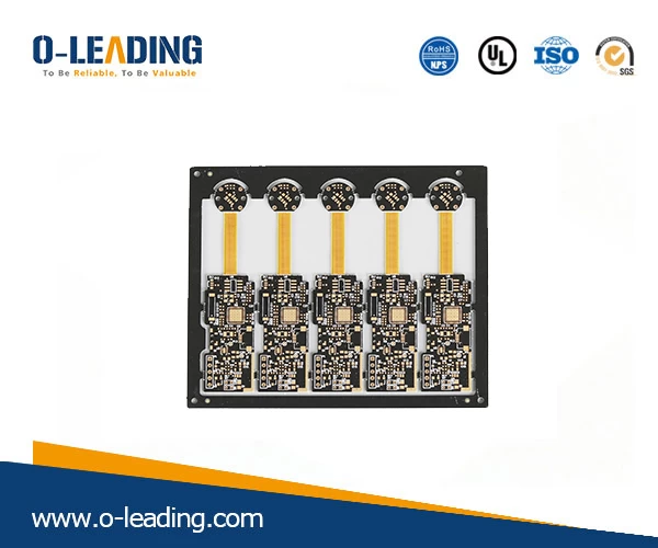
Rigid-flexible pcb factory.
Heat Dissipation (due to high thermal conductivity): for heat dissipation. Have you ever heard that some CPUs are hot enough to cook eggs, which is not an exaggeration. Most electronic components consume energy to generate heat. At this time, it is necessary to design a large area of copper foil to allow heat to be released into the air as soon as possible. Among them, not only humans can't stand it, but even electronic parts will follow.
2. Reinforcement
When using PCB reinforcement, you must have the following excellent characteristics. Most of the PCB reinforcing materials we see are made of glass fiber (GF, Glass Fiber). If you look closely, the material of glass fiber is a bit like a very thin fishing line. Because it has the following personality advantages, it is often used. When the basic material of the PCB.
High Stiffness: High "rigidity" to make the PCB not easily deformed.
Dimension Stability: Good dimensional stability.
Low CTE: Low "thermal expansion rate" to prevent the line contacts inside the PCB from coming off and causing failure.
Low Warpage: Low deformation, that is, low plate bending and plate bending.
High Modules: High "Young's Modulus"
3. Resin Matrix
The traditional FR4 plate is mainly Epoxy, and the LF (Lead Free)/HF (Halogen Free) plate is made of a variety of resins and different curing agents, which increases the cost, LF is about 20%, and HF is about 45%.
The HF plate is brittle and easy to crack and the water absorption rate becomes large. The thick plate is prone to CAF. It is necessary to use a fiber-opening cloth, a flat fiber cloth, and strengthen the impregnated material.
A good resin must have the following conditions:
Heat Resistance: Good heat resistance. After heating and welding for two to three times, it will not explode, so it is called heat resistance.
Low Water Absorption: Low water absorption. Water absorption is the main cause of PCB explosion.
Flame Retardance: Must be flame retardant.
Peel Strength: High "Tear Strength".
High Tg: High glass transition point. Most materials with high Tg are not easy to absorb water, and no water absorption is the root cause of non-explosion, not because of high Tg.
Toughness: Good "toughness". The greater the toughness, the less likely it is to explode. Toughness is also known as "destructive energy." The better the toughness of a material, the stronger its ability to withstand shock and damage.
Dielectric properties: high dielectric properties, that is, insulating materials.
4. Fillers System (powder, filler)
In the early stage of lead soldering, the temperature was not very high. The original PCB was also tolerable. Since the temperature was increased after entering the lead-free soldering, the powder was added to the PCB sheet to force the PCB to resist the temperature.
Fillers should be treated first to improve dispersion and adhesion.
Heat Resistance: Good heat resistance. After heating and welding for two to three times, it will not explode, so it is called heat resistance.
Low Water Absorption: Low water absorption. Water absorption is the main cause of PCB explosion.
Flame Retardance: Must be flame retardant.
High Stiffness: High "rigidity" to make the PCB not easily deformed.
Low CTE: Low "thermal expansion rate" to prevent the line contacts inside the PCB from coming off and causing failure.
Dimension Stability: Good dimensional stability.
Low Warpage: Low deformation, that is, low plate bending and plate bending.
Drill processibility: Difficulties in PCB drilling due to the high rigidity and high toughness of the powder.
High Modulus: Young's Modulus
Heat Dissipation (due to high thermal conductivity): for heat dissipation.