Discrimination of white pollutants in PCBA assembly welding cleaning process - cause - elimination
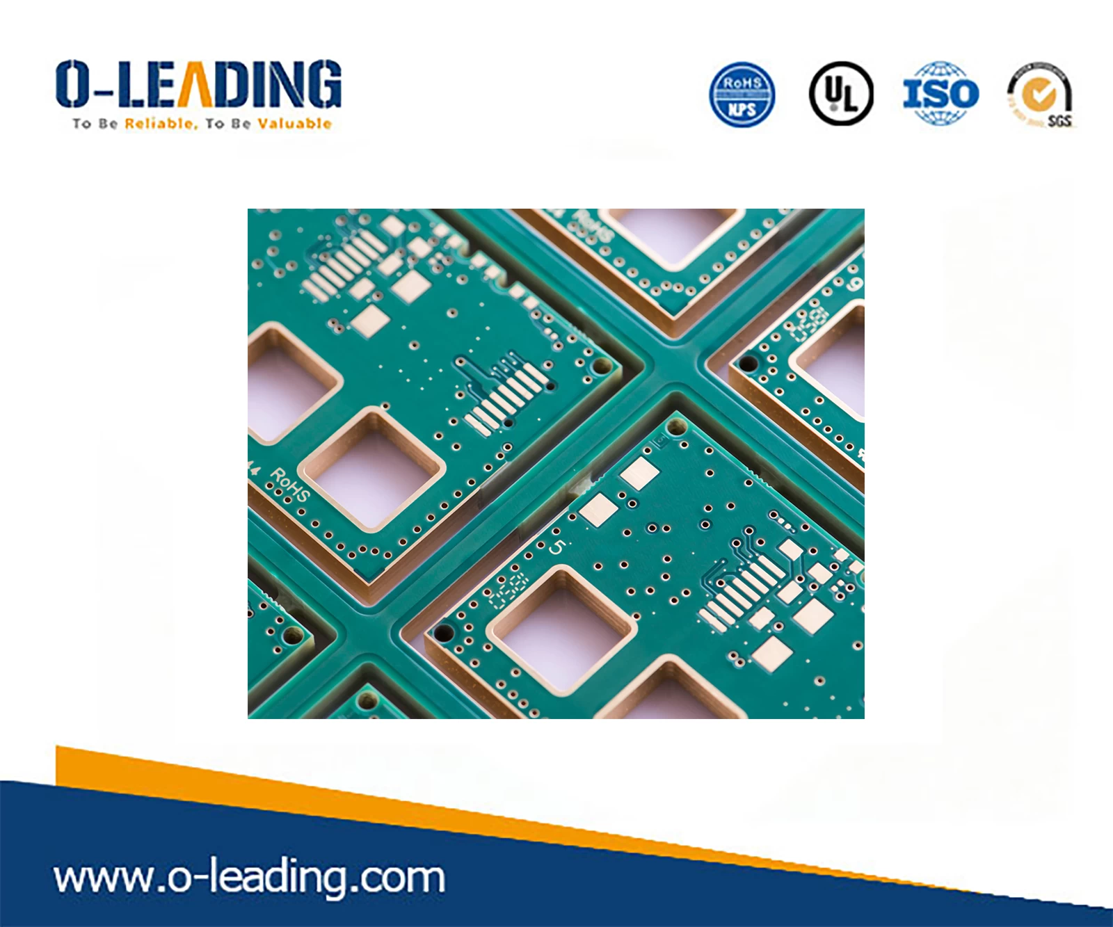
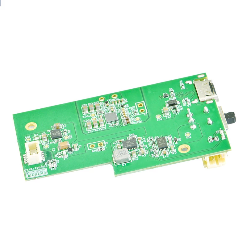
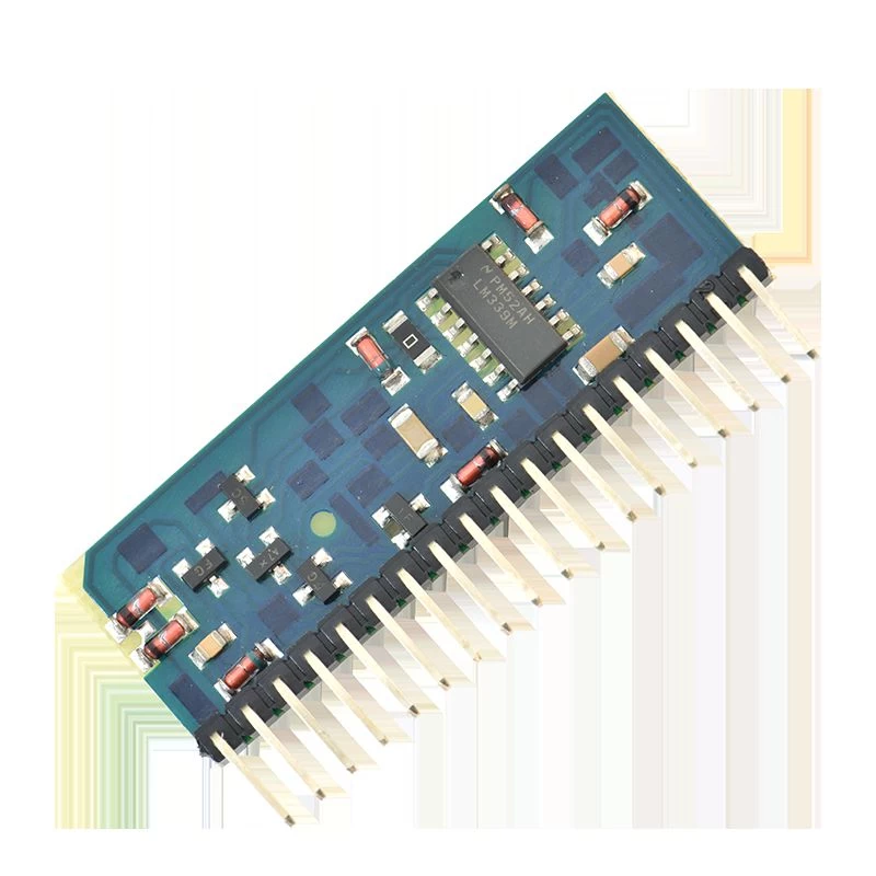
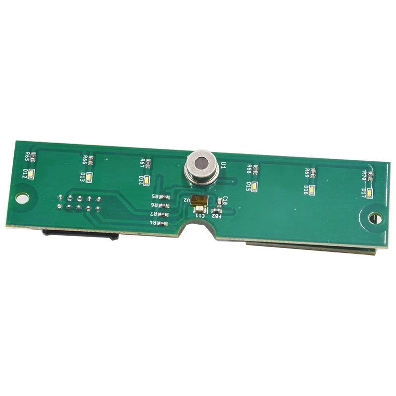
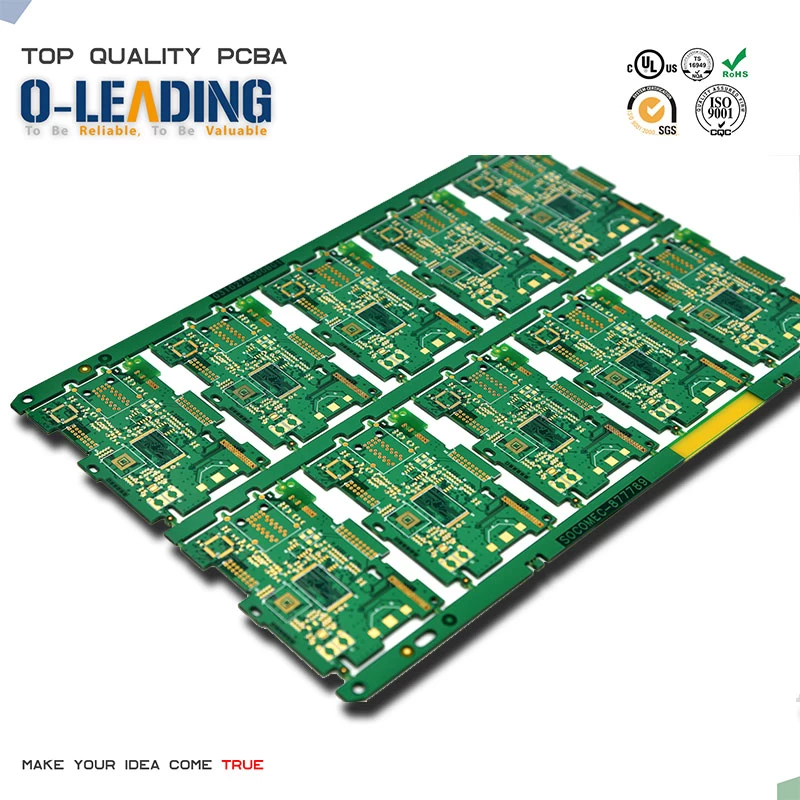
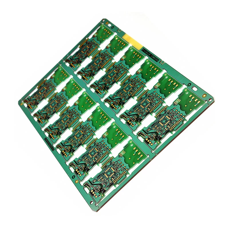
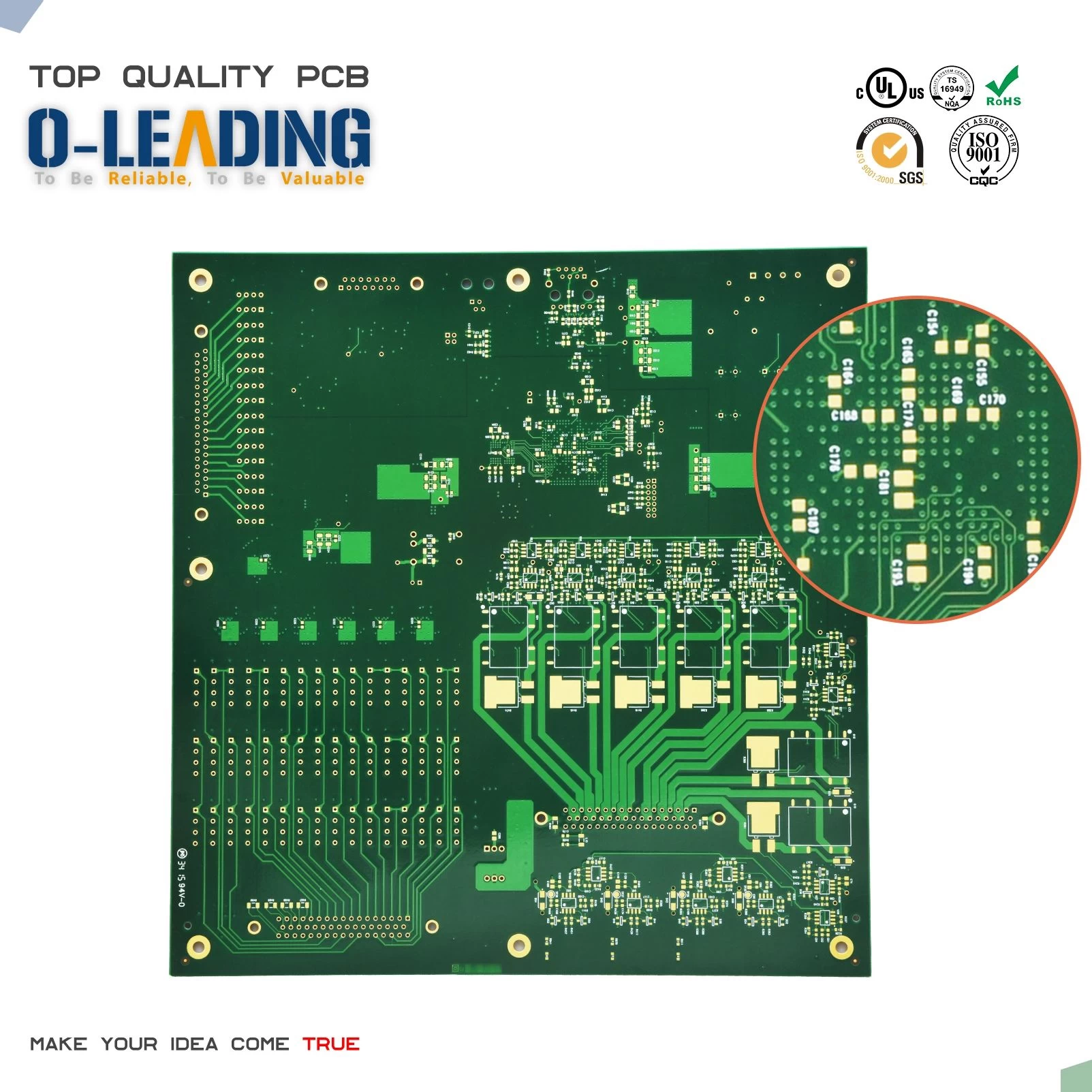
The printed circuit board assembly is the core part of the electronic product. When assembling various components, integrated circuits, chips, various electrical connectors, switches, and components on the printed circuit board assembly, flux and solder paste must be applied. Etc., after reflow, wave soldering and manual soldering, the assembly and soldering of the printed circuit board assembly can be completed.
Cleaning is an important process in PCB assembly. It plays a vital role in the quality and reliability of electronic products. It is by no means optional, or just for the sake of good looks, or simply for environmental protection.
For highly reliable electronic products, whether through through-hole or surface-mounting, no matter which process is used, after reflow, wave soldering, dip soldering or manual soldering, no matter which flux is used, including the use of After cleaning the flux, the printed circuit board assembly must be subjected to a rigorous, meticulous, and effective cleaning to remove flux residues and various contaminants. Especially for the surface assembly process and lead-free soldering technology, in high-density, high-precision assembly, cleaning can become more difficult and more important and necessary because the flux can enter the small gap between the surface-assembled component and the substrate. Teflon PCB factory china.
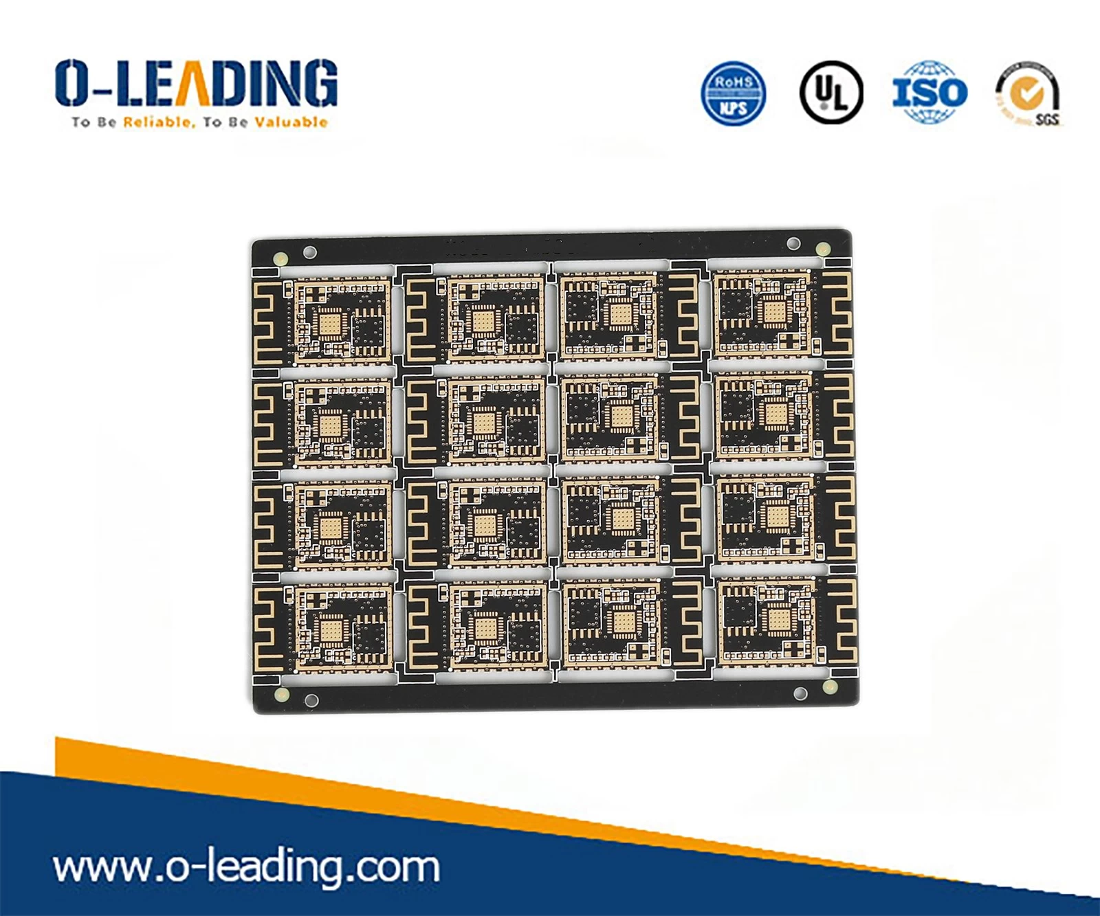
Cleaning is the process of removing contaminants. The choice of cleaning process depends not only on the type of flux, the type of impurities and the type of assembly, but also on the specific application requirements. For example, high-precision electronic instruments for aerospace, aviation, and various military equipment require extremely high reliability. In order to meet special application requirements, 2 to 3 cleaning process steps are often required.
Due to the limited number of small batches of products, most military enterprises have long been limited to manual cleaning. Cleaning agents generally use 120# aviation washing gasoline, absolute ethanol or isopropanol; this original and backward cleaning method is given to electronic products. The reliability adds many potential pitfalls.
3D printer PCB supplier.
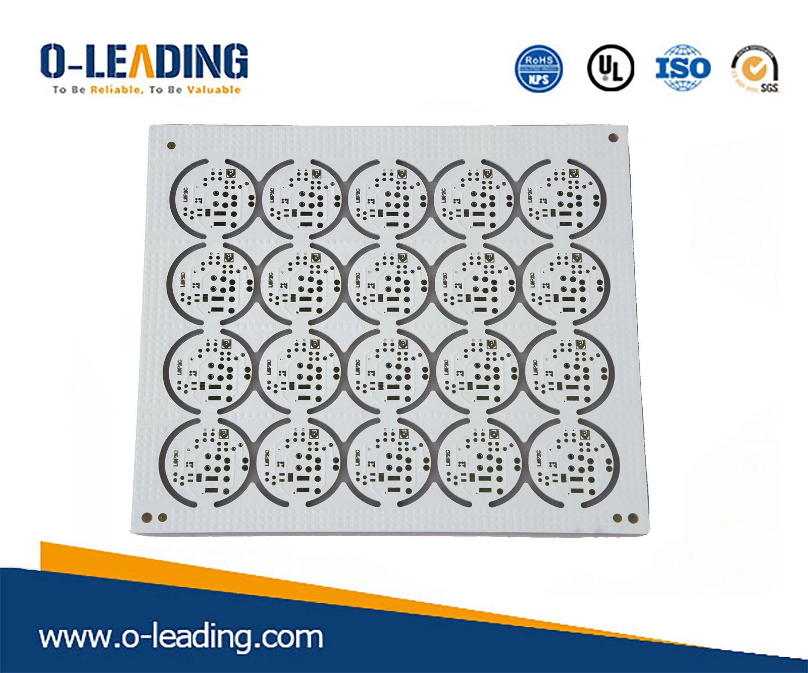
During the entire production process of the printed circuit board assembly, various contaminants will remain on the circuit board assembly and must be cleaned to ensure the reliability, working life and electrical performance of the electronic product.
The cleaning equipment and technology of the printed circuit board assembly is a system technology involving various fields of design, materials, processes and equipment.
Looking for a green environmental protection cleaning method for printed circuit board components suitable for military enterprises' scientific research and production characteristics, and discussing the incomplete cleaning, flux residues adsorbed on the surface of PCB and various pollutants on the components are necessary to study s project.
Cleaning purpose
Effectively and successfully eliminate residual contaminants after flux soldering.
2. Definition of pollutants
Any surface deposits, impurities, slag inclusions, and absorbed materials that reduce the chemical, physical, or electrical properties of a circuit, component, or component to an unacceptable level.
3. Source of pollutants
During PCB assembly, component mounting, and surface mount processes, different levels of contaminants are produced due to handling, flux usage, and soldering and production environments.

