


Summary of PCB layout rules to sum up
2. The layout should refer to the principle block diagram, and arrange the main components according to the main signal flow direction of the board.
3. The arrangement of components should be easy to debug and repair, that is, there should be no large components around the small components, the components to be debugged, and there should be enough space around the device. Laser drilling manufacturer china.
4. For the same structural circuit part, use the "symmetric" standard layout as much as possible;
5. Optimize the layout according to the standard of uniform distribution, balance of center of gravity, and beautiful layout;
6. The same type of instrumented components should be placed in one direction in the X or Y direction. The same type of polar discrete components must also strive to be consistent in the X or Y direction for ease of production and inspection.
7. The heating elements should be evenly distributed to facilitate the heat dissipation of the single board and the whole machine. Temperature sensitive components other than the temperature detecting components should be kept away from the components with large heat generation.
BACKPLANE BOARD manufacturer china.
8. The layout should try to meet the following requirements: the total connection is as short as possible, the key signal line is the shortest; the high voltage, high current signal is separated from the low current and low voltage weak signal; the analog signal is separated from the digital signal; the high frequency signal Separate from the low frequency signal; the spacing of the high frequency components should be sufficient.
9. The layout of the decoupling capacitor should be as close as possible to the power supply pin of the IC, and the loop formed between the power supply and the ground should be the shortest.
10. When placing components, it should be considered that devices using the same power supply should be placed together as much as possible to facilitate future power separation.
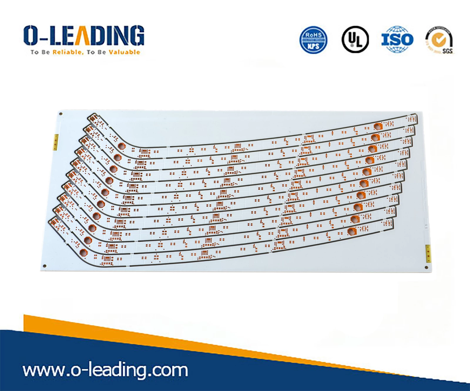
Unsymmetrical Layup Strcture.
Second, wiring
(1) Wiring priority
Key signal line priority: simulate key signal priority routing such as small signal, high speed signal, clock signal and synchronization signal
Density-Priority Principle: Start wiring from the most complex devices on the board. Wire from the densest area of the board connection
be careful:
a. Try to provide a special wiring layer for key signals such as clock signals, high-frequency signals, and sensitive signals, and ensure the minimum loop area. Manually prioritize wiring, shielding, and increasing safety clearance should be used when necessary. Guarantee signal quality.
b. The EMC environment between the power supply layer and the ground layer is poor, and signals that are sensitive to interference should be avoided.
c. The network with impedance control requirements should be routed as far as possible according to the length and line width of the line.
(2) Four specific routing methods
1. Clock wiring
The clock line is one of the most influential factors for EMC. You should make fewer holes on the clock line, try to avoid running lines with other signal lines, and keep away from the general signal lines to avoid interference with the signal lines. Also avoid the power section on the board to prevent the power supply and clock from interfering with each other.
If there is a special clock-generating chip on the board, the bottom of the chip cannot be routed. Copper should be laid underneath it, and if necessary, it can be specially cut. For many crystal oscillators with reference to the chip, these crystal oscillators should not be routed underneath, and copper isolation is required.
2. Right angle wiring
Right-angle traces are generally required to avoid PCB layout, and are almost one of the criteria for measuring the quality of the cabling. How much influence does the right-angle trace have on signal transmission? In principle, a right-angled trace will change the line width of the transmission line, causing a discontinuity in impedance. In fact, not only the right-angled lines, but also the angles and sharp-angled lines may cause impedance changes.
The effect of the right-angled line on the signal is mainly reflected in three aspects:
First, the corner can be equivalent to the capacitive load on the transmission line, slowing down the rise time;
Second, the impedance discontinuity will cause signal reflection;
The third is the EMI generated by the right angle tip.
3. Differential routing
Differential signal (Differential Signal) is widely used in high-speed circuit design. The most critical signal in the circuit often adopts differential structure design. Definition: In layman's terms, the driver sends two equal values and inverts. The signal, the receiving end determines whether the logic state is "0" or "1" by comparing the difference between the two voltages. The pair of traces carrying the differential signals is called a differential trace.