


Method for preventing warpage of PCB board during manufacturing process
A, the arrangement of the interlayer prepreg should be symmetrical, for example, a six-layer board, the thickness between the layers of 1 to 2 and 5 to 6 and the number of sheets of the prepreg should be the same, otherwise it is easy to warp after lamination.
B, multi-layer core sheets and prepregs should use the same supplier's products.
C, the line pattern area of the outer A side and B side should be as close as possible. If the A side is a large copper surface and the B side is only a few lines, the printed board is easily warped after etching. If the line areas on both sides are too different, add a separate grid on the thin side to balance.
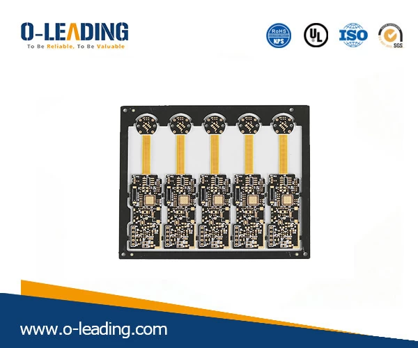
Flex-Rigid PCB factory china.
2, before baking the baking sheet:
The copper plate is pre-baked (150 degrees Celsius, 8±2 hours). The purpose is to remove the moisture in the plate and completely cure the resin in the plate to further eliminate the residual stress in the plate. Help. At present, many double-sided and multi-layer boards still adhere to the step of pre- or post-bake. However, there are some exceptions for sheet metal. At present, the time regulations for baking sheets of PCB factories are also inconsistent, from 4-10 hours. It is recommended to decide according to the grade of the printed board produced by the customer and the customer's requirements for warpage. After cutting into a jigsaw and drying it, the whole piece of material is baked and then unloaded. Both methods are feasible. It is recommended to dry the plate after cutting. The inner panel should also be baked.
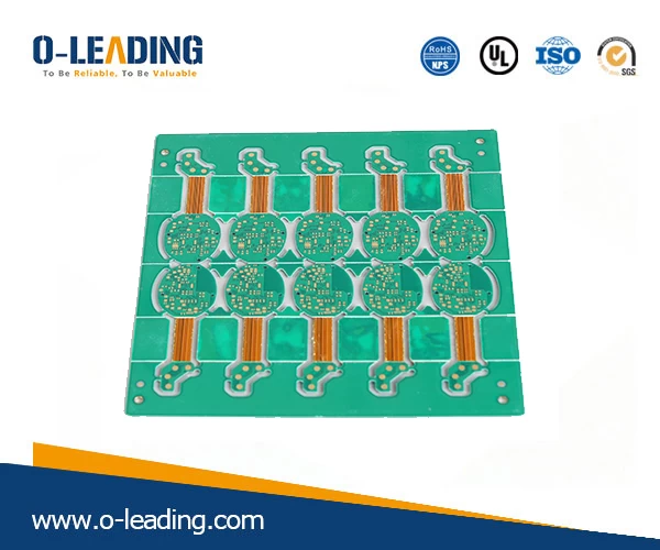
Rigid-flexible PCB with ENIG.
3. The warp and weft of the prepreg:
The warp and weft shrinkage rates of the prepreg are different after lamination, and the warp and weft directions must be separated when cutting and laminating. Otherwise, it is easy to cause warpage of the finished board after lamination, even if it is pressed, it is difficult to correct. The reason for the warpage of the multi-layer board is that the latitude and longitude of the prepreg is not separated when it is laminated, and it is caused by the disorder.
How to distinguish the warp and latitude? The rolled prepreg is wound in the warp direction and the width direction is the weft direction; for the copper foil sheet, the long side is in the weft direction and the short side is the warp direction. If it is not certain, it can be inquired to the manufacturer or supplier.
Rigid-flexible pcb factory.
4. After stress removal after lamination:
The multi-layer board is taken out after hot pressing and cold pressing, sheared or milled off the burrs, and then baked in an oven at 150 ° C for 4 hours to gradually release the stress in the sheet and completely cure the resin. This step cannot be omitted.
5, the plate needs to be straightened when plating:
When the 0.4-0.6mm ultra-thin multi-layer board is used for plate surface plating and pattern plating, special nip rolls should be made. After the thin plate is clamped on the flying plate of the automatic plating line, the clip on the whole flying bar is used with a round stick. The rollers are strung together to straighten all the plates on the roll so that the plate after plating does not deform. Without this measure, after plating a copper layer of twenty or thirty microns, the sheet would bend and be difficult to remedy.
6. Cooling of the board after hot air leveling:
When the hot plate of the printed board is leveled, it will be impacted by the high temperature of the solder bath (about 250 degrees Celsius). After being taken out, it should be placed on the flat marble or steel plate for natural cooling, and sent to the post-processing machine for cleaning. This is good for the board to prevent warpage. In some factories, in order to enhance the brightness of the lead-tin surface, the hot air of the board is put into the cold water immediately after being leveled. After a few seconds, it is taken out for post-treatment. This kind of hot and cold impact is likely to cause warping on some types of boards. Curved, layered or blistering. In addition, an air floating bed can be installed on the equipment for cooling.
7, the treatment of warping board:
Jeddah pcb, the printed board will be 100% flatness inspection during the final inspection. All unqualified boards will be picked out, placed in an oven, baked at 150 degrees Celsius and under heavy pressure for 3 to 6 hours, and naturally cooled under heavy pressure. Then, the plate is taken out by pressure relief, and the flatness is checked. This saves some of the boards, and some of the boards need to be pressed two to three times to level. The Shanghai Huabao agent's pneumatic plate warping straightening machine has a very good effect in remediating the warpage of the circuit board by the use of Shanghai Bell. If the above-mentioned anti-warping process measures are not implemented, some of the board drying pressure is useless and can only be scrapped.