


PCB shielding cover design points
The width of the mask cover is generally 0.6mm----0.8mm
The length of the mask of the shield is generally 3 - 5mm, generally about 5mm, otherwise it is too scattered.
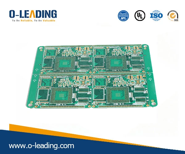
The pad spacing of the shield is generally 1mm. Multilayer PCB manufacturer in china.
Note that the welding feet of the shield are the Great Wall feet, and the length can be as long as the pads. The requirements here are not high.
The hardware engineer, according to the above method, then he will keep the component gap of 0.3 mm above the pad gap of the component pad, and plug the component inside.
High Tg PCB manufacturer china.
When calculating the height of the shield, it is sufficient to draw the height of the component according to the maximum tolerance of the highest component. It is not necessary to leave the thickness of the solder paste. Because the thickness of the stencil is only 0.1mm, the component is not attached, and the solder paste is 0.1. Mm is high, and after the components are attached, the components are still trapped inside the solder paste. In addition, the height of the components is basically made according to the difference. Then, according to the gap between the top surface of the highest component and the inner surface of the shield, 0.2 is taken. Mm, so calculate the height of the shield can be.
AOI Testing supplier china.
Shielding is the separation of metal between two spatial regions to control the induction and radiation of electric, magnetic and electromagnetic waves from one region to another. Specifically, the shield is used to surround the components, circuits, assemblies, cables, or interference sources of the entire system to prevent interference with electromagnetic fields. The shields are used to surround the receiving circuits, devices, or systems to prevent them from being exposed to the outside world.
The influence of electromagnetic fields. Because the shield absorbs energy (eddy current loss), reflected energy (interface reflection of electromagnetic waves on the shield) and cancels energy (electrical waves) from external electromagnetic waves and internal electromagnetic waves from wires, cables, components, circuits or systems. The magnetic induction generates a reverse electromagnetic field on the shielding layer, which can cancel the effect of partially interfering electromagnetic waves, so the shielding body has the function of reducing interference.