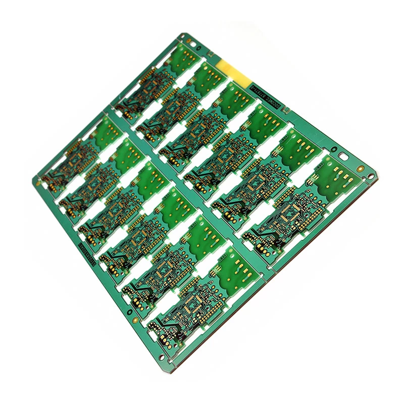
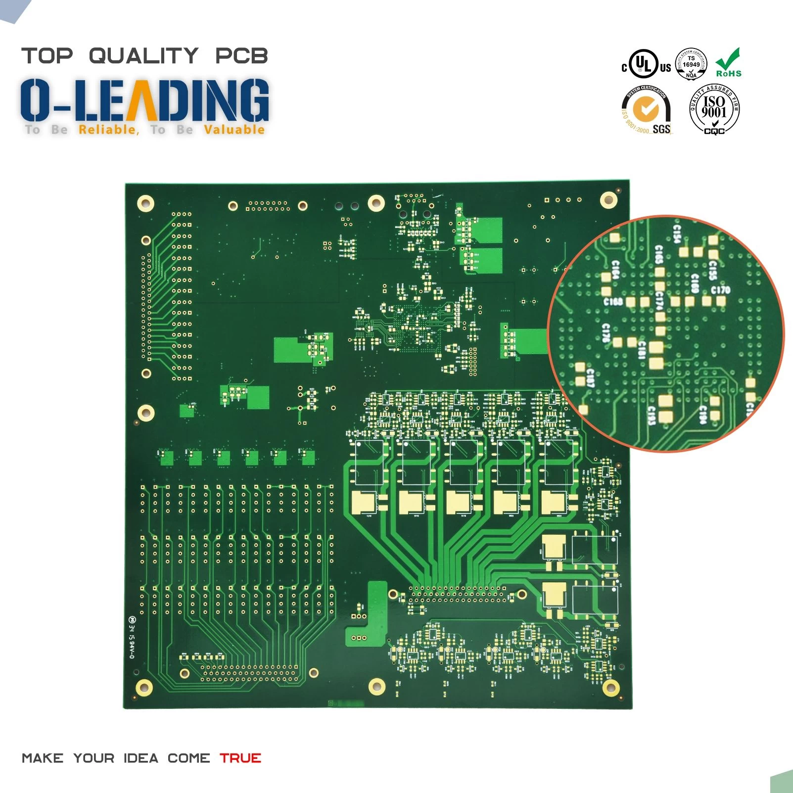
How many layers of PCB design is best? I will read the meaning of each layer of the PCB.
Layer in PCB design
01
Mechanical Layers
Mechanical layers are generally used to place instructive information about the board and assembly methods, such as PCB dimensions, dimensional markings, data sheets, via information, and assembly instructions.
02
Prohibit the wiring layer (Keep Out Layer)
Used to define areas on the board where components and wiring can be placed efficiently. A closed area is drawn in this layer as the effective area of the wiring, and it is not automatically laid out and routed outside the area.
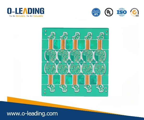
03
Silkscreen layer
The silk screen layer is a text layer, which belongs to the top layer in the PCB and is generally used for annotation.
(1) Top Overlay (Top Overlay)
Used to mark the projected outline of the component, the label of the component, the nominal value or model number, and various comment characters.
(2) Bottom Screening (Bottom Overlay)
Same as the top silkscreen layer, if all the labels are included in the top silkscreen layer, the underlying silkscreen layer can be closed.
04
Solder Mask
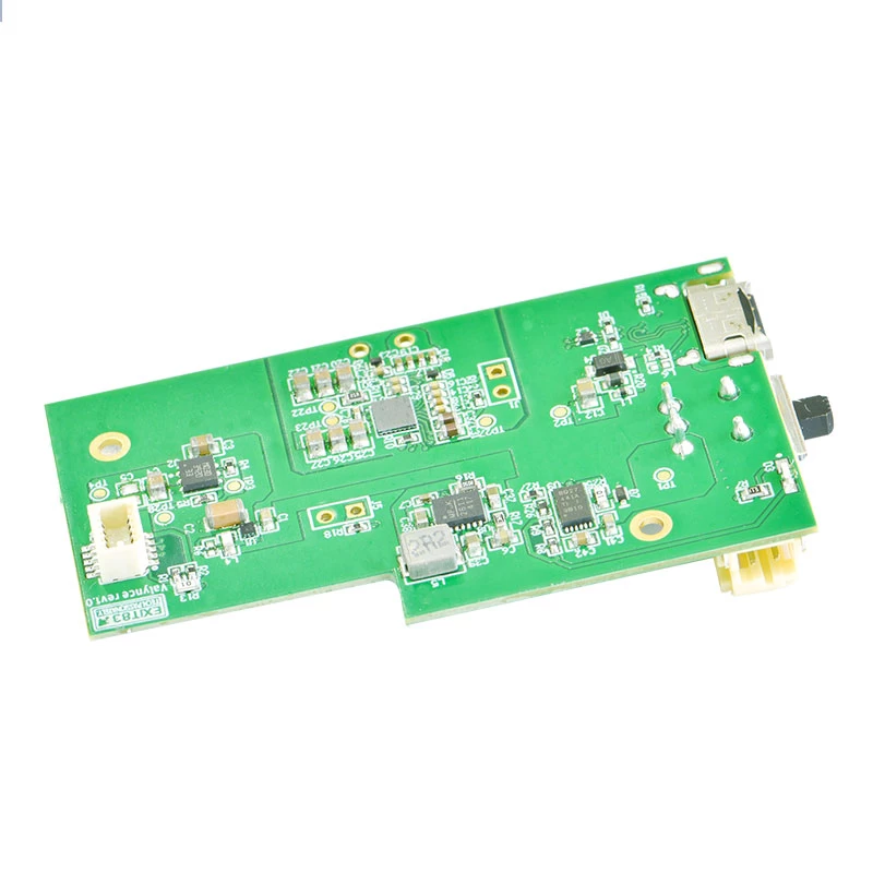
The solder mask refers to the portion of the printed circuit board to which green oil is applied. In fact, this solder mask uses the negative output, so after the shape of the solder mask is mapped to the board, it is not the green oil solder mask, but the copper skin is exposed.
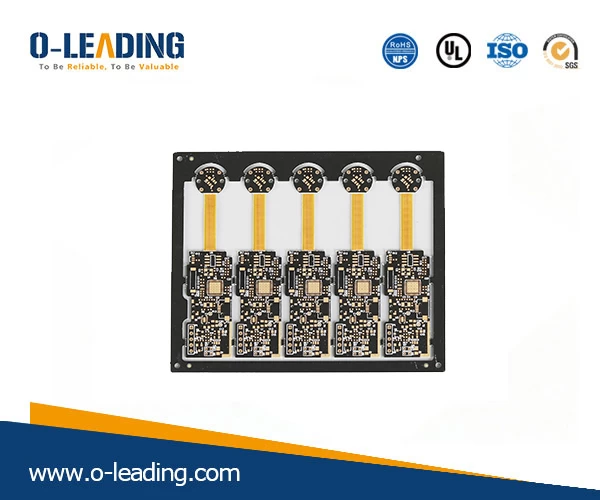
05
Multi Layer
The pads and through vias on the board penetrate the entire board and establish electrical connections with different conductive pattern layers, so the system has an abstract layer - multiple layers. Generally, the pads and vias are placed on multiple layers. If this layer is turned off, the pads and vias cannot be displayed.
06
Drill Layer
The drilled layer provides drilling information during the manufacturing process of the board (such as pads and vias that require drilling).
07
Signal Layers
(1) Top layer signal layer (Top Layer)
Also called component layer, mainly used to place components, for double-layer boards and multi-layer boards can be used to arrange wires or copper.
(2) Bottom signal layer (Bottom Layer)
Also known as solder layer, mainly used for wiring and soldering, for double-layer boards and multi-layer boards can be used to place components.
(3) Intermediate signal layer (Mid-Layers)
There are up to 30 layers, which are used to lay out signal lines in the multi-layer board. Power lines and ground lines are not included here.
08
Internal Power Plane (Internal Planes)
Usually referred to as the inner layer, it only appears in the multi-layer board. The number of layers of the PCB board generally refers to the sum of the signal layer and the inner layer. Similar to the signal layer, the inner and inner layers, the inner layer and the signal layer can be connected to each other through through holes, blind holes and buried holes.

