


What are the restrictions on PCB baking?
Conditions for PCB baking:
At present, the industry generally sets the conditions and time for PCB baking as follows:
1. The PCB is well sealed within 2 months of the manufacturing date. After unpacking, it should be placed in an environment with temperature and humidity control (≦ 30 ℃ / 60% RH, according to IPC-1601) for more than 5 days. Bake at 120 ± 5 ℃ for 1 hour.
2. The PCB is stored for 2 to 6 months beyond the manufacturing date, and it needs to be baked at 120 ± 5 ℃ for 2 hours before going online.
3. The PCB is stored for 6 to 12 months beyond the manufacturing date, and it needs to be baked at 120 ± 5 ℃ for 4 hours before going online.
4. PCBs are stored for more than 12 months beyond the date of manufacture. Basically, it is not recommended to use them, because the bonding force of multi-layer boards will age with time, and quality problems such as product instability may occur in the future. Probability, and the production process also has the risk of bursting and poor tin eating. If you have to use it, it is recommended to bake it at 120 ± 5 ℃ for 6 hours. Before a large number of trials, you should print a few pieces of solder paste and put into production to ensure that there are no solderability problems before continuing production.
Another reason not to use PCBs that have been stored for a long time is because the surface treatment will gradually fail over time. For ENIG, the industry's shelf life is 12 months. After this time limit, depending on the immersion layer, Depending on the thickness, if the thickness is thinner, the nickel layer may appear in the gold layer due to diffusion and form oxidation, which affects the reliability. It is not inadvertent.
5. All baked PCBs must be used within 5 days, and unprocessed PCBs must be baked at 120 ± 5 ℃ for another hour before going online.
Stacking method when PCB is baked:
1. When baking large-sized PCBs, use a flat stack. It is recommended that the maximum number of stacks should not exceed 30 pieces. Open the oven to remove the PCB within 10 minutes after baking. Anti-plate bending fixture. Large-size PCB is not recommended for vertical baking, and it is easy to bend.
2. When baking small and medium-sized PCBs, you can use horizontal stacking. The maximum number of stacks is recommended not to exceed 40 pieces. It can also be upright. The number is unlimited. Open the oven and remove the PCB within 10 minutes after baking. Allow it to cool, and press the anti-plate bending fixture after baking.
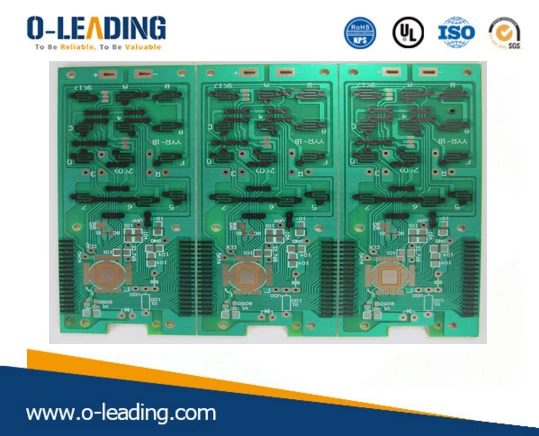
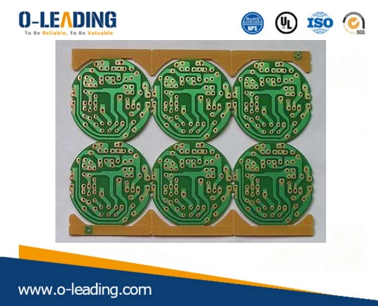
Mobile Phone PCB supplier china
PCB baking recommendations:
1. It is recommended to just bake PCB with a temperature of 105 ± 5 ℃, because the boiling point of water is 100 ℃, as long as it exceeds its boiling point, water will become water vapor, because the water molecules contained in PCB will not be too It does not need too high temperature to increase the rate of gasification. Too high temperature or gasification speed will easily cause rapid expansion of water vapor, which is actually detrimental to quality, especially for multilayer boards and those with buried holes. PCB, 105 ℃ is just above the boiling point of water, the temperature will not be too high, it can dehumidify and reduce the risk of oxidation. Moreover, the ability of the oven temperature control has been improved a lot than before.
2. Whether the PCB needs to be baked depends on whether its packaging is wet, that is, whether the HIC (Humidity Indicator Card) in the vacuum packaging has been shown to be wet. If the packaging is good, HIC does not indicate that it is wet. You can go online without baking.
3. It is recommended to use the "upright" and spaced baking for PCB baking, because this can achieve the maximum effect of hot air convection, and the moisture can be easily baked out of the PCB. However, for large-sized PCBs, it may be necessary to consider whether the vertical type will cause board bending deformation problems.
4. After the PCB is baked, it is recommended to place it in a dry place and allow it to cool quickly. It is best to press the "anti-plate bending jig" on the top of the board, because the general object from the high heat state to the cooling process will easily absorb moisture However, rapid cooling may cause plate bending, which must strike a balance.
Disadvantages of PCB baking and things to consider:
1. Baking will accelerate the oxidation of the PCB surface coating, and the higher the temperature, the longer the baking, the more unfavorable.
2. It is not recommended to bake the board with OSP surface treatment at high temperature, because the OSP film will degrade or fail due to high temperature. If you have to do baking, it is recommended to use a temperature of 105 ± 5 ℃, which should not exceed 2 hours, and it is recommended to use it within 24 hours after baking.
3. Baking may have an impact on the formation of IMC, especially for HASL (spray tin) and ImSn (chemical tin, dip tin) surface treatment boards, because the IMC layer (copper-tin compound) was already in the PCB stage. Generated, that is, generated before PCB soldering, but baking will increase the thickness of the IMC that has been generated on this layer, causing reliability issues.