


Via design in high speed PCB
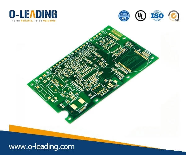
(1) Select a reasonable via size. For multi-layer general-density PCB designs, vias of 0.25mm/0.51mm/0.91mm (hole/pad/POWER isolation) are preferred; for some high-density PCBs, 0.20mm/0.46 can also be used. For mm/0.86mm vias, try not to use vias; for vias with power or ground, consider using larger sizes to reduce impedance; Lead free HASL wholesales china.
(2) The larger the POWER isolation area, the better. Consider the density of the via hole on the PCB, which is generally D1=D2+0.41.
(3) The signal traces on the PCB should not be changed as much as possible, that is, the vias should be minimized;
(4) The use of a thinner PCB facilitates reducing the two parasitic parameters of the via;
(5) The power and ground pins should be close to the vias. The shorter the leads between the vias and pins, the better, because they will lead to an increase in inductance. At the same time, the power and ground leads should be as thick as possible to reduce the impedance; Immersion Gold manufacturer china.
(6) Place some ground vias near the vias of the signal-changing layer to provide a short-distance loop for the signal.
In addition, the via length is also one of the main factors affecting the via inductance. For vias used for top and bottom conduction, the via length is equal to the PCB thickness. Due to the increasing number of PCB layers, the PCB thickness often reaches more than 5 mm.
However, in the design of high-speed PCBs, in order to reduce the problems caused by vias, the via length is generally controlled within 2.0 mm.
For vias with a via length greater than 2.0 mm, the via resistance continuity can be improved to some extent by increasing the via aperture. When the via length is 1.0 mm or less, the optimum via hole diameter is 0.20 mm to 0.30 mm.