


Some minor principles of PCB technology
The minimum width of the printed wire is related to the amount of current flowing through the wire:
1: The line width is too small, the resistance of the printed wire is large, and the voltage drop on the line is large, which affects the performance of the circuit.
If the line width is too wide, the wiring density is not high, and the board area is increased. In addition to increasing the cost, it is also disadvantageous for miniaturization.
If the current load is calculated at 20 A/mm 2 , when the thickness of the copper clad is 0.5 MM, (generally so much), the current load of 1 MM (about 40 MIL) line width is 1 A. Multilayer PCB manufacturer in china.
Therefore, the line width of 1-2.54MM (40--100MIL) can meet the general application requirements, the ground wire and power supply on the high-power equipment board, according to the power size, the line width can be appropriately increased, while the number in the low power On the circuit, in order to improve the wiring density, the minimum line width can be satisfied by taking 0.254 - 1.27MM (10 - 15MIL).
In the same circuit board, the power line. The ground line is thicker than the signal line.
3D printer PCB supplier.
2: Line spacing: When it is 1.5MM (about 60MIL), the insulation resistance between lines is greater than 20M ohms, and the maximum withstand voltage between lines can reach 300V. When the line spacing is 1MM (40MIL), the maximum withstand voltage between lines is 200V. Therefore, on a circuit board with medium and low voltage (line voltage not greater than 200V), the line spacing is 1.0--1.5MM (40--60MIL). In low-voltage circuits, such as digital circuit systems, it is not necessary to consider the breakdown voltage. Production process allows, can be small.
3: Pad:
For a 1/8W resistor, a pad lead diameter of 28 MIL is sufficient.
For 1/2W, the diameter is 32MIL, the lead hole is too large, and the width of the pad copper ring is relatively reduced, resulting in a decrease in the adhesion of the pad. It is easy to fall off, the lead hole is too small, and the component is difficult to play.
4: Draw circuit border:
The shortest distance between the frame line and the component pin pad can't be less than 2MM (usually 5MM is reasonable), otherwise it is difficult to cut.
5: Component layout principles:
A General principle: In the PCB design, if the circuit system has both digital and analog circuits and high-current circuits, it must be laid out separately, so that the matching between the systems can be minimized in the same type of circuit, according to signal flow and function. , block, partition and place components.
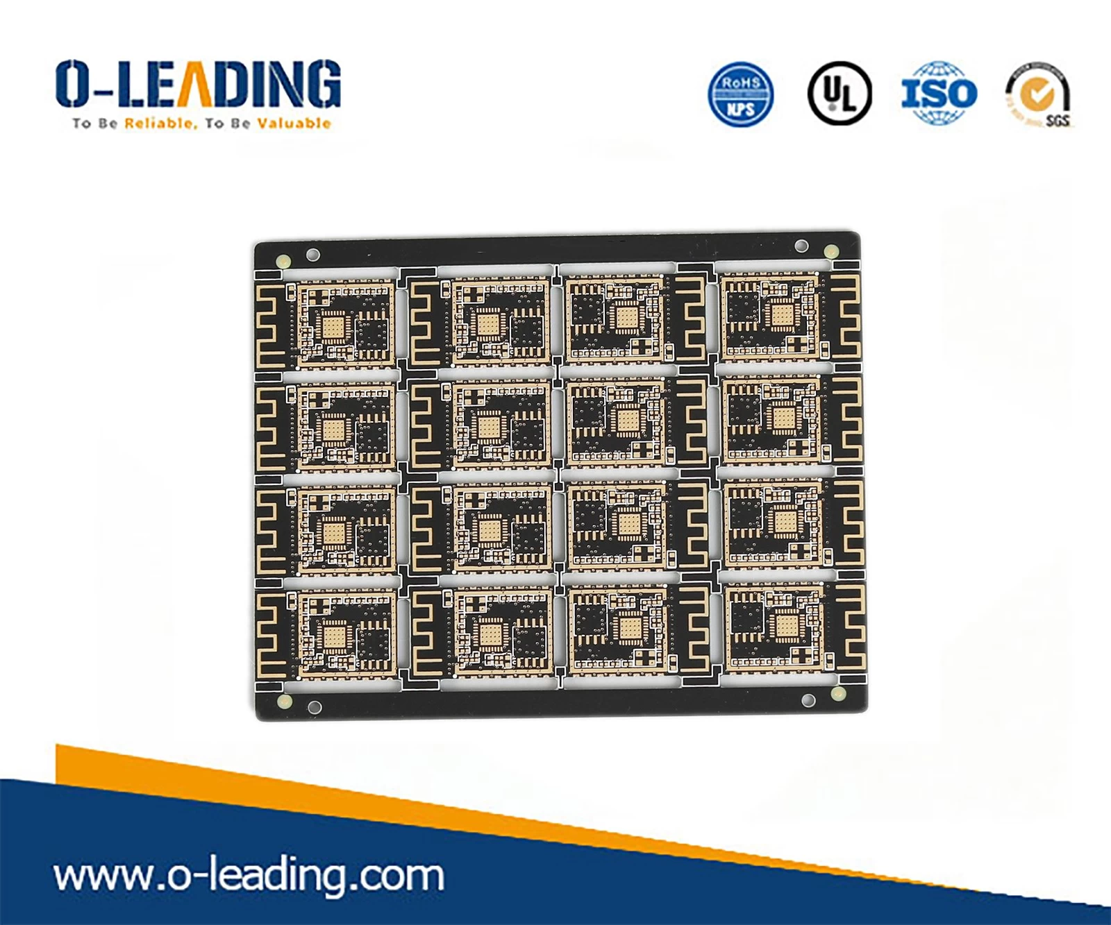
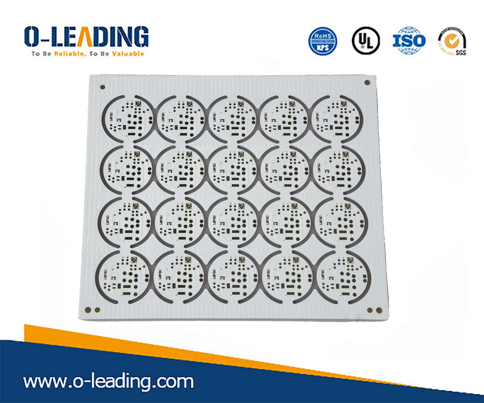
Printed circuit boards supplier.
B: Input signal processing unit, the output signal driving component should be close to the edge of the board, so that the input and output signal lines are as short as possible to reduce the interference of input and output.
C: Component placement direction: Components can only be arranged in both horizontal and vertical directions. Otherwise, they must not be used in plug-ins.
D: component spacing. For medium density boards, small components, such as small power resistors, capacitors, diodes, etc., the spacing between discrete components is related to the plug-in, soldering process. When soldering, the component spacing can be 50-100 MIL (1.27-- 2.54MM) can be larger by hand, such as 100MIL, integrated circuit chip, component spacing is generally 100--150MIL
E: When the potential difference between components is large, the component spacing should be large enough to prevent discharge.
F: In the IC, the tantalum capacitor is close to the power supply of the chip. Otherwise, the filtering effect will be worse. In the digital circuit, in order to ensure the reliable operation of the digital circuit system, the power supply in each digital integrated circuit chip and Place the IC between the ground to remove the tantalum capacitor.
The tantalum capacitor is generally made of ceramic capacitor. The capacity is 0.01~0.1UF. The choice of tantalum capacitor capacity is generally selected according to the reciprocal of the system operating frequency F. In addition, at the entrance of the circuit power supply A 10UF capacitor is also required between the power and ground lines, and a 0.01UF ceramic capacitor.
G: The hour hand circuit component is as close as possible to the clock signal pin of the MCU chip to reduce the length of the connection of the clock circuit. It is better not to trace the line below.